Spanish
  Chinese
  Russian
  German
  French
  Japanese
  Portuguese
  Hindi
Hindi Research Article, Res J Opt Photonics Vol: 1 Issue: 1
Broadband Plasmonic Total Light Absorption in an Aldoped ZnO/spacer/silver Stack Patterned with Graded Photonic Super-crystal
Murthada Adewole1, David Lowell1, Safaa Hassan1, David George1, Hualiang Zhang2, Jingbiao Cui3 and Yuankun Lin2,4*
1Department of Physics, University of North Texas, Denton TX 76203, USA
2Department of Electrical and Computer Engineering, University of Massachusetts Lowell, Lowell, MA 01854, USA
3Department of Physics & Materials Science, University of Memphis, Memphis, TN 38152, USA
4Department of Electrical Engineering, University of North Texas, Denton, TX 76203, USA
*Corresponding Author : Yuankun Lin, PhD
Department of Physics, University of North Texas, Denton, TX 76203, USA
Tel: (940) 565-4548
E-mail: yuankun.lin@unt.edu
Received: October 07, 2017 Accepted: October 14, 2017 Published: October 20, 2017
Citation: Adewole M, Lowell D, Hassan S, George D, Zhang H, et al. (2017) Broadband Plasmonic Total Light Absorption in an Al-doped ZnO/spacer/silver Stack Patterned with Graded Photonic Super-crystal. Res J Opt Photonics 1:1.
Abstract
For the first time, Al-doped ZnO patterned with graded photonic super-crystals with dual lattice and dual period and stacked on SiO2/ silver films, has been studied for plasmonic total light absorption. Broadband total light absorption occurs due to the gradient size distribution of dot disks in the photonic lattice. Localized surface plasmon polaritons (SPPs) are selectively confined in certain dot disks following the SPP formation condition, and total light absorption happens when the SPPs are coupled to the Fabry–Pérot resonance which is dependent on the spacer thickness.
Keywords: Total light absorption; Fabry–Perot resonance; Surface plasmon polariton; Al-doped ZnO
Introduction
Total light absorption (TLA) (or perfect absorption) and plasmonic TLA with zero reflection and zero transmission in thin film stacks and metal-insulator-metal (MIM) stacks have been studied for applications in photodetectors, solar energy harvesting, among other things [1-13]. In patterned MIM stacks, light can easily couple with surface plasmons to form surface plasmon polaritons (SPPs) following momentum conservation [1,4,5,8]. Plasmonic TLA has been observed in MIM stacks without strict conditions for the material selections, as is the case for thin film stacks [1-8]. In the infrared wavelength range, indium tin oxide (ITO), Ga-doped ZnO, and Al-doped ZnO (AZO) are good candidates for plasmonic materials due to their low optical loss and thermally, electrically, or optically tunable optical properties [14-22]. These materials have used to realize tunable plasmonic TLA [14-22].
TLA in broad wavelength is desired for applications such as solar energy harvesting. Multiplexed plasmon resonances in metal duallattices [4,5,23] have been used to achieve broadband plasmonic TLA. Dual lattice photonic crystals can be used to generate broadband light trapping enhancement for solar energy harvesting [24-26]. Simulations have shown that the light extraction efficiency is greatly enhanced if the cathode of an organic light emitting diode is patterned with gradient photonic super-crystals (GPSCs) [27].
In this paper, for the first time, we have simulated the light reflection from AZO/glass spacer/silver stacks that are patterned with a newly discovered GPSC with dual lattice and dual period. The gradient size distribution of dot disks in the GPSC lattices provide many choices for the formation of localized SPPs. Electric field intensity simulations illustrate the selection condition of localized SPPs and plasmonic TLA is explained in terms of SPPs coupling with Fabry–Pérot (F-P) resonance.
Simulation Methods
In the simulation, AZO is patterned with a GPSC within the AZO/ glass/silver stack. The GPSC is formed by eight-beam interference (two sets of four interfering beams) [27,28]. One set of beams has a cone angle, α, and the same intensity, I1, and their wavevectors can be written as: k(sin(α)cos(45°), sin(α)sin(45°), cos(α)), k(-sin(α) cos(45°), sin(α)sin(45°), cos(α)), k(sin(α)cos(45°), -sin(α)sin(45°), cos(α)), k(-sin(α)cos(45°), -sin(α)sin(45°), cos(α)). The other set of beams has a cone angle, β, (with α>β) with equal intensities, I2, and the following wavevectors: k(sin(β)cos(45°), sin(β)sin(45°), cos(β)), k(-sin(β)cos(45°), sin(β)sin(45°), cos(β)), k(sin(β)cos(45°), -sin(β) sin(45°), cos(β)), k(-sin(β)cos(45°), -sin(β)sin(45°), cos(β)). The intensity ratio of the beams, I1/I2, is 5:1 in the simulation with zero initial phase. When these eight beams interfere, a pattern with dual lattice and dual period is formed. To an approximation, the large period is determined by the small cone angle β and the small period is related to the large cone angle α. The small period is determined by the equation, P1=2π/Δk, where Δk is the difference in wavevector between two adjacent beams with cone angle α. A unit super-cell of 12P1×12P1 (or P3×P3) of the interference pattern is shown in Figure 1a. Three periods are shown in the figure. ![]() and the large period P3=12P1. These different periods (P1, P2, and P3) help couple light from free space to the GPSC pattern following the conservation of momentum. Two sets of lattices (dual lattices) can be identified by the yellow and blue squares although the size of the dots on the vertices of the square are graded. The size of the dots in one set of the lattices indicated by the yellow square become smaller as we move from the edge to the central region, while the dot size becomes bigger for the lattice indicated by the blue square.
and the large period P3=12P1. These different periods (P1, P2, and P3) help couple light from free space to the GPSC pattern following the conservation of momentum. Two sets of lattices (dual lattices) can be identified by the yellow and blue squares although the size of the dots on the vertices of the square are graded. The size of the dots in one set of the lattices indicated by the yellow square become smaller as we move from the edge to the central region, while the dot size becomes bigger for the lattice indicated by the blue square.

Figure 1: (a) Graded photonic super-crystals with dual lattice as indicated by the yellow and blue squares and dual period. (b) Cross-section of the AZO/ glass/silver stack. (c) Simulated reflection spectra from the AZO/glass/silver stack patterned with a square lattice photonic crystal (yellow triangles) and with the graded photonic super-crystals (blue circles). (d) Simulated reflection spectra from the AZO/glass/silver stack patterned with graded photonic supercrystals for different spacer thicknesses of 700, 620, 600, 560, 500 and 450 nm.
The interference pattern I(r) was compared with threshold intensity. When I(r)< Ith the pattern becomes air, and AZO when I(r)> Ith. The dielectric function of the AZO was obtained through characterization of an AZO film by spectroscopic ellipsometry in our previous paper [29]. The thickness of the AZO and silver layers in the AZO/glass/silver stack, as shown in Figure 1b in cross-section, were both set to be 100 nm, and the glass thickness was adjusted to search for TLA. The absorption (A) is related to the transmission (T) and reflection (R) by A=1-T-R. The transmission is zero due to the silver mirror. Thus, in the simulation, the reflection from the AZO/ glass/silver stack was simulated and plotted. A=100% when T=R=0. The simulations of reflection spectra were performed with a finitedifference time-domain (FDTD) method, using MIT’s open source software package, MEEP [30]. The polarization of light source is in the [0,1] direction. Due to the large unit cell size, all simulations were performed on the Simpetus Electromagnetic Simulation Platform in Amazon Web Services (AWS). Parallel computations were used in 36-core virtual machines in AWS.
Results and Discussions
Figure 1c shows TLA for the AZO/glass/silver stack where the AZO has been patterned with a traditional single square lattice and a GPSC with dual lattice as in Figure 1a. The reflection dip is much wider in the spectrum from the AZO patterned with the GPSC than that of the AZO patterned with the single square lattice. In order to understand the TLA mechanism, further simulations were performed for AZO/glass/silver stacks with different spacer thicknesses, and AZO pattern period P1. Figure 1d shows the reflection at different spacer thicknesses. At a thickness of 700 nm, no TLA is observed. When the thickness is decreased, the reflection dip wavelength is blue-shifted and the reflection at the dip wavelength becomes smaller. When the glass spacer thickness=550 nm, TLA is observed in the range of 3055 and 3298 nm. When the thickness is decreased further, the reflection at the dip wavelength becomes non-zero as seen for the case of thickness=450 nm. Thus, TLA is related to the glass spacer thickness.
Figures 2a and 2b shows the electric field intensity in the x-y plane just above the silver layer and below the AZO layer, respectively. The red circles in Figures 2a and 2b indicate the edge of one set of lattices with large diameters (the lattice indicated by the blue square in Figure 1a. As shown in the figure, the strong electric field is confined near the lattice with large diameters and weak near the second lattice with small diameters. The electric field is strong in the central region and weak near the edge of the unit super-cell, as seen in Figures 2a and 2b. This indicates that the SPP is localized and the gradient dot disk size is responsible for the broadband plasmonic TLA. Due to the polarization in the [0,1] direction, the electric field is very strong in y direction near the edges of lattice dots (top and bottom edges in the top view in Figure 2b and below the AZO down to the silver layer. The cross-section view of the electric field intensity in x-z plane cutting through the dashed blue line (center of the dots), dashed yellow line (edge of the dots), and dashed white line in Figure 2b, is shown in Figures 3c1, 3c2 and 3c3), respectively. In the glass spacer, the electric field intensity in Figure 2c2 is stronger near silver layer and weaker near AZO layer while the electric field intensity in Figure 2c1 is stronger near the AZO layer and weaker near silver layer. The TLA can be considered a result of the coupling between SPPs and Fabry-Pérot (F-P) resonance in an up-down or zig-zag path in the space as shown in Figure 2c4.

Figure 2: Simulated electric field intensity in the spacer layer (a) just above the silver layer and (b) just below AZO for AZO/spacer/silver stack patterned with GPSC. The solid circles duplicate the location of one set of lattices indicated by the blue square in Figure 1a. (c1, c2, c3) Cross-section views of the simulated E-field intensities cutting through the dashed blue, yellow, and white lines in (b). (c4) A schematic showing the zig-zag Fabry-Pérot path inside the glass spacer.
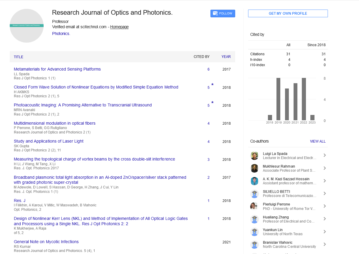
The following condition will be met for the formation of SPPs at the interface of the AZO and glass spacer:
 (1)
(1)
 (2)
(2)
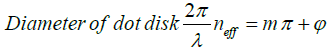
Where λ is the wavelength, m an integer number, neff the effective refractive index as defined in Eq. (2), εAZO and εs the dielectric constants of AZO and spacer, respectively. For m=2 and diameters 840 and 940 nm, SPP wavelengths of 3037 and 3269, respectively, can be obtained from the Eq. (1), compared with the broadband plasmonic TLA in the range of 3055 and 3298 nm from the reflection spectra. From Figure 1a, the measured sizes for the largest and second largest dot disks are 914 and 822 nm, respectively. It is the dot area where strong electric field confinement appears, as in Figures 2a and 2b. Thus the gradient size of dot disks contributes to the broad TLA.
Further simulations have been performed to assess the TLA wavelength dependence on the period P1. The results are shown in Figure 3. When the period decreases as seen in Figure 3a, the TLA wavelength decreases following Eq. (1) and Eq. (2). On the other hand, the TLA wavelength increases as the period increases, as seen in Figure 3c. The glass spacer thickness was also changed to 500, 600, and 650 nm for the periods of 800, 1200, and 1400 nm, respectively, in order to realize plasmonic TLA. Broadband TLA occurs at 2866- 3088, 3003-3230, and 3336-3504 nm, for periods of 800, 1200, and 1400 nm, respectively, as seen in Figures 3a, 3b, and 3c. Based on the optical paths of up-down or zig-zag as shown in Figure 2c4, F-P resonance wavelengths can be estimated to be in the range of 2757- 2994, 3021-3327, and 3491-3576 nm for GPSCs with periods of 800, 1200, and 1400 nm, respectively. These wavelength ranges are close to the simulated TLA wavelength ranges, indicating a coupling of SPPs with F-P resonance between the patterned AZO and silver films. Further tests of the above hypothesis are performed using the GPSC with a period P1 of 1400 nm as described below.

Figure 3: Simulated total light absorption in AZO/glass/silver stack for three different periods of the graded photonic super crystals: 800 nm (a), 1200 nm (b), and 1400 nm (c) with spacer thicknesses of 500, 600, and 650 nm, respectively.
Using Eq. (1) and Eq. (2) with period P1 of 1400 nm and dot disk sizes between 960 and 1040 nm, SPP wavelengths were calculated between 3317 and 3517 nm. These disk sizes were used for the calculation of the F-P resonance wavelength above. However, the dot disks with sizes of 960 and 1040 nm in diameter in GPSC with a period P1 of 1400 nm are no longer in the central region of the unit super-cell. Thus the electric field simulation is performed in AZO/ spacer/silver stack patterned with GPSC with a period P1=1400 nm and a spacer thickness of 650 nm, as shown in Figure 4. The electric field intensities in the x-y plane at a location just above the silver, between the silver and AZO, and just below the AZO are shown in Figures 4a, 4b and 4c, respectively. From these figures, we can see that strong electric fields are confined in eight dot disks in row #2, ten dot disks in row #3, and four dot disks in row #4. Thus most of the electric field is confined in dot disks with sizes of 67.4% and 74.0% of period P1 for row #2 and #3, respectively. P1=1400 nm thus these sizes are 944 and 1036 nm, respectively, in good agreement with the predicted dot disk sizes of 960 and 1040 nm based on Eq. (1) and Eq. (2).

Figure 4: Simulated electric field intensity in the spacer layer (a) just above the silver layer, (b) between the silver and AZO, and (c) just below AZO for AZO/ spacer/silver stacks patterned with GPSC with spacer thickness of 650 nm. The solid circles duplicate the location of one set of lattices indicated by the blue square in Figure 1(a). The numbers in (c) are the percentage of dot disk size relative to the period P1 in different rows.
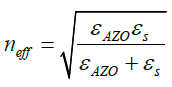
The coupling of SPPs with F-P resonance is further tested and the tunability of TLA is simulated. When a negative bias is applied onto AZO, a carrier accumulation occurs in a thin layer of AZO near the AZO/spacer interface. The carrier distribution can be solved by Poisson’s equation [21]. The change of carrier concentration results in a change of plasma frequency for AZO, as described by Eq. (3).
 (3)
(3)
where e is the electron charge, m* the effective mass, and ε0 is the electric permittivity of vacuum. The change in plasma frequency will lead to a change in the AZO permittivity.
Figure 5 shows the results of simulations of plasmonic TLA in AZO/spacer/silver stacks when the plasma frequency of a 10 nm layer of AZO near the AZO-glass interface is changed from 1.45 eV to 1.65 eV and 2.20 eV while the rest of the AZO (90 nm) keeps the original plasma frequency of 1.45 eV. The stack is patterned with GPSC with a period P1=1000 nm and has a spacer thickness of 560 nm. For a plasma frequency of 1.65 eV, localized SPPs around the dot disk with smaller size than the one in Figure 2a can participate in coupling with the F-P resonance thus the TLA dip wavelength is shifted as seen in the Figure 5. At a plasma frequency at 2.20 eV, localized SPPs occur but are not coupled to the F-P resonance. This simulation indicates the tunability of plasmonic TLA through changes in carrier concentration. A real device can be designed with air holes in AZO for connection to an electrical source.

Figure 5: Simulated total light absorption in AZO/glass/silver stacks for three plasma frequencies in a 10 nm AZO layer near the AZO/glass interface while the rest of the 90 nm AZO has a plasma frequency of 1.45 eV.
Conclusion
Broadband plasmonic TLA has been observed in the simulations of reflection from AZO/spacer/silver stacks patterned with a GPSC with dual period and dual lattice. The TLA broadening is caused by the gradient size distribution of dot disks in the patterned AZO. TLA occurs when the localized SPPs are coupled with the F-P resonance in the spacer.
Acknowledgement
This work is supported by research grants from the U.S. National Science Foundation under Grant Nos. CMMI- 1661842, 1661749, and ECCS-1407443.
References
- Aydin K, Ferry EV, Briggs MR, Atwater HA (2011) Broadband polarization-independent resonant light absorption using ultrathin plasmonic super absorbers. Nat Commun 2: 517.
- Luk TS, Fofang NT, Cruz-Campa JL, Frank I, Campione S (2014) Surface plasmon polariton enhanced ultrathin nano-structured CdTe solar cell. Opt Express 22: A1372-A1379.
- Chen H (2012) Interference theory of metamaterial perfect absorbers. Opt Express 20: 7165-7172.
- Zhang B, Hendrickson J, Guo J (2013) Multispectral near perfect metamaterial absorbers using spatially multiplexed plasmon resonance metal square structures. J Opt Soc Am B 30: 656-662.
- Hendrickson J, Guo JB, Zhang WB, Soref R (2012) Wideband perfect light absorber at midwave infrared using multiplexed metal structures. Opt Lett 37: 371-373.
- Fang Z, Zhen YR, Fan L, Zhu X, Nordlander P (2012) Tunable wide-angle plasmonic perfect absorber at visible frequencies. Phys Rev B 85: 245401.
- Nielsen MG, Pors A, Albrektsen O, Bozhevolnyi, SI (2012) Efficient absorption of visible radiation by gap plasmon resonators. Opt Express 20: 13311-13319.
- Kim W, Simpkins BS, Long, JP, Zhang B, Hendrickson J, et al. (2015) Localized and nonlocalized plasmon resonance enhanced light absorption in metal-insulator-metal nanostructures. J Opt Soc Am B 32: 1686-1692.
- Sun T, Guo CF, Cao F, Akinoglu EM, Wang Y, et al. (2014) A broadband solar absorber with 12 nm thick ultrathin a-Si layer by using random metallic nanomeshes. Appl Phys Lett 104: 251119.
- Sturmberg BCP, Chong TK, Choi DY, White TP, Botten LC, et al. (2016) Total absorption of visible light in ultrathin weakly absorbing semiconductor gratings. Optica 3: 556-562.
- Kats MA, Blanchard R, Genevet P, Capasso F (2013) Nanometer optical coatings based on strong interference effects in highly absorbing media. Nat Mater 12: 20-24.
- Kats MA, Byrnes SJ, Blanchard R, Kolle M, Genevet P, et al. (2013) Enhancement of absorption and color contrast in ultra-thin highly absorbing optical coatings. Appl Phys Lett 103: 101104.
- Long Y, Su R, Wang Q, Shen L, Li B, et al. (2014) Deducing critical coupling condition to achieve perfect absorption for thin-film absorbers and identifying key characteristics of absorbing materials needed for perfect absorption. Appl Phys Lett 104: 091109.
- Campione S, Kim I, de Ceglia D, Keeler GA, Luk TS (2016) Experimental verification of epsilon-near-zero plasmon polariton modes in degenerately doped semiconductor nanolayers. Opt Express 24: 18782-18789.
- Luk TS, Campione S, Kim I, Feng S, Jun YC, et al. (2014) Directional perfect absorption using deep subwavelength low-permittivity films. Phys Rev B 90: 085411.
- Yoon J, Zhou M, Badsha MA, Kim TY, Jun YC, et al. (2015) Broadband epsilon-near-zero perfect absorption in the near-infrared. Sci Rep 5: 12788.
- Kim TY, Badsha MA, Yoon J, Lee SY, Jun YC, et al. (2016) General strategy for broadband coherent perfect absorption and multi-wavelength all-optical switching based on epsilon-near-zero multilayer films. Sci Rep 6: 22941.
- Zhu C (2016) SiO2/bi-layer GZO/Ag structures for near-infrared broadband wide-angle perfect absorption. J Phys D Appl Phys 49: 425106.
- Cleary JW (2016) Tunable short-to mid-infrared perfectly absorbing thin films utilizing conductive zinc oxide on metal. Opt Mater Express 5: 1898-1909.
- Pradhan AK (2014) Extreme tunability in aluminum doped zinc oxide plasmonic materials for near-infrared applications. Sci Rep 4: 6415.
- George D, Li L, Lowell D, Ding J, Cui J, et al. (2017) Electrically tunable diffraction efficiency from gratings in Al-doped ZnO. Appl Phys Lett 110: 071110.
- Kinsey N (2015) Epsilon-near-zero Al-doped ZnO for ultrafast switching at telecom wavelengths. Optica 2: 616-622.
- Chenggang H, Liyuan L, Zeyu Z, Xu’nan C, Xiangang L (2009) Mixed plasmons coupling for expanding the bandwidth of near-perfect absorption at visible frequencies. Opt Express 17: 16745-16749.
- Callahan DM, Horowitz KA, Atwater HA (2013) Light trapping in ultrathin silicon photonic crystal superlattices with randomly-textured dielectric incouplers. Opt Express 21: 30315-30326.
- Rinnerbauer V (2014) Superlattice photonic crystal as broadband solar absorber for high temperature operation. Opt Express 22: A1895.
- Rinnerbauer V (2015) Nanoimprinted superlattice metallic photonic crystal as ultraselective solar absorber. Optica 2: 743.
- Hassan S, Lowell D, Lin Y (2017) High light extraction efficiency in organic light-emitting diodes by patterning the cathode in graded superlattice with dual periodicity and dual basis. J Appl Phys 121: 233104.
- Lowell D, Lutkenhaus J, George D, Philipose U, Chen B, et al. (2017) Simultaneous direct holographic fabrication of photonic cavity and graded photonic lattice with dual periodicity, dual basis, and dual symmetry. Opt Express 25: 14444-14452
- George D, Li L, Jiang Y, Lowell D, Mao M, et al. (2016) Localized surface plasmon polariton resonance in holographically structured Al-doped ZnO. J Appl Phys 120: 043109.
- Oskooi AF, Roundy D, Ibanescu M, Bermel P, Joannopoulos JD, et al. (2010) MEEP: A flexible free-software package for electromagnetic simulations by the FDTD method. Compu Phys Commun 181: 687-702.