Research Article, J Polym Sci Appl Vol: 2 Issue: 1
Structural and Thermal Treatment Evaluation of Electrospun PVDF Nanofibers for Sensors
Adrian Parker1, Akira Ueda2, Marvinney CE3, Hargrove SK1, Frances Williams1 and Richard Mu1,4*
1TIGER Institute, Tennessee State University, Nashville TN 37209, USA
2Center for Physics and Chemistry of Materials, Fisk University, Nashville TN 37208, USA
3Interdisciplinary Material Science Program, Vanderbilt University, Nashville TN 37235, USA
4Department of Biomedical Engineering, Vanderbilt University, Nashville TN 37235, USA
*Corresponding Author : Richard Mu
TIGER Institute, Tennessee State University, Nashville TN 37209, USA
Tel: 615-519-3370
E-mail: rmu@tnstate.edu; rich.mu@gmail.com
Received: December 01, 2017 Accepted: January 18, 2018 Published: January 24, 2018
Citation: Parker A, Ueda A, Marvinney CE, Hargrove SK, Williams F, et al. (2018) Structural and Thermal Treatment Evaluation of Electrospun PVDF Nanofibers for Sensors. J Polym Sci Appl 2:1.
Abstract
Polyvinylidene fluoride (PVDF) polymer has seen increased use in industrial, energy harvesting, and sensor applications due to its chemical inertness, durability, flexibility, and, more importantly,
its ferroelectric properties. Decreases in fabrication scale have increased PVDF sensor capabilities dramatically. Nanofibers fabricated by electro spinning provide an increased surface area over that of amorphous thin films, and thus have a greater sensitivity to measurements collected; analysis is required, however, to ascertain changes made in the sensor capabilities as temperatures increase. We have fabricated PVDF nanofibers by an electro-spinning process and annealed the samples at temperatures ranging from 40oC to 100oC. Scanning electron microscopy (SEM) imaging was performed before and after heat treatment, and confocal Raman analysis was also performed after treatment. Analysis of the SEM micrographs indicated no changes in morphology, while the Raman spectroscopy showed increases in both spectral intensity and beta to alpha phase ratio, which directly affects ferroelectric capabilities. Nanofibers showed greater stability than what has been achieved in PVDF thin films at similar temperatures.
Keywords: Polyvinylidene fluoride; Nanofibers; Electro spinning; Pyroelectric sensors
Introduction
Polyvinylidene fluoride (PVDF) has been used in film and membrane form since the 1980s as distillation and contactor elements, in addition to other industrial applications. It can act as wastewater treatment membranes due to high mechanical strength and chemical resistance and as biomedical and bio-separation components due to its pure polymer nature [1]. Of greater interest, however, are its piezo-, pyro-, and ferroelectric properties. In its crystalline form, PVDF can exist in α, β, δ, and γ phases, with the β phase being most desirable due to spontaneous polarization. Thicker wafers allow the pyroelectric capabilities to be utilized; the most common use is the mapping, profiling, and alignment of lasers [2]. Thin films are typically coated on both sides with nickel, copper, or aluminum in order to conduct and collect generated electrical energy, or provide measurements of voltage changes caused by mechanical deformations. These deformations and changes in the strain in the PVDF allow its piezoelectric nature to be utilized by way of measuring the changes in pressure. Films have also been studied for use as adaptive smart sensing films for high-resolution space mirror applications to combat weight limitations in space-based telescope systems [3]. In addition, micro patterned films have allowed the pyroelectric functionality to harvest waste heat from temperature fluctuations in devices.
As the size scale of fabricated PVDF has decreased, sensor capabilities have increased dramatically. Nanofibers fabricated by electro spinning provide a higher surface area than that of amorphous thin films, which gives greater sensitivity to measurements collected. The pulling process of electro spinning also promotes a higher concentration of β phase in the fibers. These parameter changes are particularly important for chemical gas sensors; the higher surface area available for measurements directly affects performance features such as sensitivity and selectivity of gases. Gas sensor electrodes coated with nanofiber membranes have been shown to have sensitivity four times greater than that of standard quartz crystal microbalance sensors. The technology has been applicable to acoustic wave sensors, resistive gas sensors, photoelectric gas sensors, and optical gas sensors [4]. Nanofibers have also advanced energy harvesting in the realm of wearable composites in items such as gloves and shoes [5].
Recently PVDF nanofibers have been studied as a separator material in the lithium ion battery environment, mainly for their increased thermal stability and resistance to shrinkage, which leads to short circuits in standard polyethylene (PE) separators [6,7]. The porosity of PE is lost at its melting temperature of 135°C, but the chemical and thermal reactions that lead to thermal runaway events (the cause of fires and explosions in the battery environment) actually begin at 90°C [8]. There are currently no systems available to monitor conditions within a single battery cell; management systems at the battery pack level rely on state-of-charge (SOC) measurements, which are a combination of power fade, capacity fade, instantaneous available power, and average temperature measurements [9,10]. The pyroelectric capabilities of PVDF present an opportunity to collect localized temperature data and implement an early warning system in the battery environment if a suitable sensor setup can be found. The present work studies the integrity of the β phase and of the physical structure of the nanofibers under temperature changes in the window of the battery environment. This window is applicable to piezo- and pyroelectric sensor capabilities in all fields and environments.
Experimental
Materials
Commercial PVDF powder was purchased from Sigma- Aldrich Chemical. The powder has a density of 1.74 g/mL at 25°C and average molecular weight of 534,000 by GPC. It also has glass and melt transition temperatures of -38°C and 171°C, respectively. Acetone and dimethylformamide (DMF) were purchased from Fisher Chemical. The solvents have assay percentage ranges of 99.5% and 99.8% respectively, and meet current American Chemical Society (ACS) specifications.
Solution preparation and electro-spinning
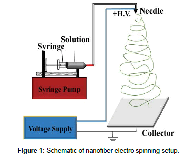
Nanofibers for the study were fabricated using an electro spinning process. The PVDF solution consisted of a 12% weight amount of PVDF powder, combined with a 60:40 ratio by volume mixture of DMF and acetone as a solvent. The ingredients were mixed at 45°C for 12 hours. Before electro spinning, the solution was mixed again at 45°C for one hour to ensure solution homogeneity. Upon completion of the heated stirring process, the PVDF solution was loaded into a syringe. The syringe was then placed in a syringe pump at a 4.5 mL/ hr flow rate and connected by tube to an 18-gauge needle. The needle was connected to a 14.5 kV power supply, which was then grounded at a 15 cm aluminum collector plate. The distance between the needle tip and the collector plate was set at 18 cm. Solution exited the needle tip in viscous drop form until initiation of the voltage, at which point the electric field generated by the applied high voltage began to pull the suspended drop of polymer solution into nanofiber form. The PVDF was deposited at the collector plate as a single continuous fiber in the form of a non-woven mat. Schematic illustration of the electro spinning setup is shown in Figure 1. The electro spinning methodology was adapted from the experimental setup utilized by Dan Li et al. [11]. Silicon wafers were utilized as deposition substrates for analysis of nanofiber uniformity. Lithium ion battery anodes consisting of graphite electrodes coated on copper film current collectors were used as substrates for nanofiber depositions to be used in phase concentration analysis.
Scanning electron microscopy
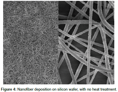
The ZEISS SEM MERLIN imaging system at the Vanderbilt Institute of Nanoscale Science and Engineering (VINSE) facility, located at Vanderbilt University, was used to collect SEM measurements. The system consists of an electron optical column, specimen chamber, and control panel. The column system is a GEMINI II, which houses a Schottky field emitter used as an electron gun. The column also includes a beam booster and combined electrostatic/ electromagnetic lens doublet. The specimen chamber contains a fiveaxis motorized stage for x-, y-, and z-direction movements, as well as tilt and rotation. All measurements utilized the In-Lens detector, a high-resolution detector that picks up signals directly in the path of the electron beam. Silicon wafers with nanofiber depositions are shown in Figure 2.
Raman Spectroscopy
Nanofiber deposition was made on seven battery anodes for 60 seconds each, after which the samples were annealed at 40°C, 50°C, 60°C, 70°C, 80°C, 90°C, and 100°C, all for one hour. Raman spectra were collected from each sample on a grid background consisting of five rows and ten columns that spanned the entire surface of the anode for total of 50 collected spectra per sample. Grid schematic and anode samples before and after electro spinning deposition are shown in Figure 3.
All Raman measurements taken for the study utilized a HORIBA Jobin Yvon LabRAM HR800 integrated Raman system; the system consists of a microscope confocally coupled to an 800-millimeter focal length spectrograph. Measurements were taken using a diode pumped 532-nanometer laser source with a power setting of 100 milliwatts (mW). Approximately 66% of the laser power was attenuated by the system for a power of 33-34 mW at the sample. Raman measurements were taken using a 200-micrometer (μm) aperture and a 1,800 grating. Spectra were collected in the frequency range of 200-1,500 wave number (cm-1), with collection settings of eight-second exposures, eight repetitions, 100X magnification, and a D0.3 laser filter setting Figure 4.
Results and Discussion
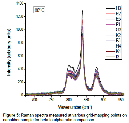
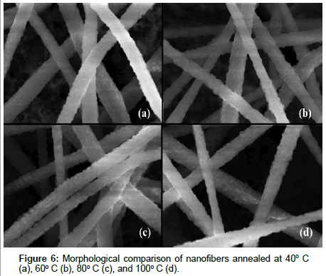
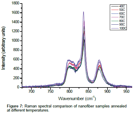
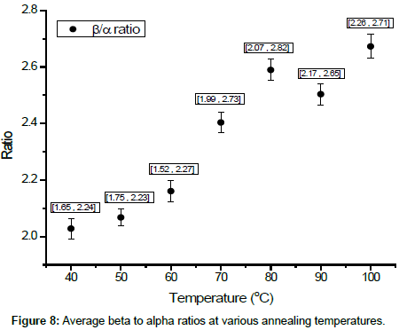
The SEM micrographs were used to examine the physical characteristics of the electrospun nanofibers before heat treatment with global and local views. A careful survey of the overall deposited surface shows that it is very uniform throughout the entire region of 5 square inch area. Figure 5 displays the Raman spectra collected over the sample grid indicated in Figure 3. There is no structural component change throughout the samples even though there are overall Raman intensity variations from spot to spot on the grid, as discussed in the following section. Heat treatment from room temperature (as deposited) to 100°C showed no clear morphological changes as per Figure 6. Figure 7 represents the averaged Raman spectra upon thermal treatment on the anode. To illustrate the effects of heat treatment on α and β phase in the nanofibers, the intensity ratio of the Raman peaks at 794 cm-1 and 839 cm-1 were calculated as shown in Figure 8 [13,14].
The properties and potential applications of PVDF polymer have been actively investigated by us and others [15-19]. Like many other polymers, the physical structure as a bulk material and/or at the molecular level can be very different, depending on the specific process used for material preparation [16,17]. Careful and detailed experimental planning and parameter control are critical to obtaining meaningful information from the PVDF materials. It is known that electrospun PVDF nanofibers are ferroelectric and contain 20 - 30% more β phase in volume compared to the commercially available piezoelectric PVDF sheets from Measurement Specialty, for example. It is also known that the piezoelectric properties of PVDF can be lost over time and with temperature, which impedes wide device and sensory applications of this material. The recent study of a piezoelectric PVDF thin film with nondestructive second harmonic generation laser spectroscopy shows that the piezoelectric properties will be lost near the temperature of 90 –100°C for the “clamped” film; the free-standing film, on the other hand, will lose its piezoelectric properties as the temperature increases and the film shrinks [19]. Thus, the study of heat treatment of PVDF nanofibers is an important first step towards sensing phenomena such as potentially dangerous temperature changes in lithium ion battery cells.
In order to obtain reliable and reproducible results, we have conducted detailed SEM imaging and Raman measurements as described in the experimental section and shown in Figures 4 and 5 for as-prepared samples. The direct SEM observation of PVDF nanofibers shows no obvious morphology changes with temperature, suggesting that thermal annealing at temperatures below 100°C causes no major structural transformation. On the other hand, the Raman spectral intensity associated with β and α phase peak intensity has increased with annealing temperature. It clearly suggests that thermal annealing has resulted in more β phase conversion either at the expense of α phase or amorphous phase. In either case, the results are somewhat surprising, and show promise for PVDF as a piezoelectric and pyroelectric sensor.
It is believed that the increase in β to α phase ratio is more than likely due to the fact that the thermal annealing process may have provided additional activation energy for the as-deposited nanofibers to form more β phase, since the electrospun nanofibers are stretched during the electro-spinning process and the temperature is too low for PVDF to form a larger β phase crystal. This hypothesis is consistent with the Raman results obtained from the thermal annealing temperatures.
In summary, we have carried out a post thermal annealing study on electrospun PVDF nanofibers using SEM imaging and confocal Raman analysis. The results show 1) electrospun PVDF nanofibers have a higher volume fraction of β phase and the potential to have higher piezoelectricity, and 2) unlike piezoelectric PVDF film, the thermal annealing of the deposited nanofibers are stable up to 100°C and results in even more β phase. Thus thermal annealed nanofibers may be even more piezoelectric and pyroelectric for sensory applications.
Acknowledgement
Authors gratefully acknowledge financial supports from NEEC: N00174- 16-C-0008, Office of Naval Research Grant #: N00014-17-1-3060, ARO: W911NF-15-1-0441 NSF: CMMI-1462329, Title III-HGBI P031B090214, and VINSE.
References
- Liu F, Hashim, Liu Y, Abed MRM, Li K (2011)Progress in the Production and Modification of PVDF Membranes. J Membrane Sci 375: 1-27.
- G. Toci, Mazzoni M(2000) Use of a PVDF Pyroelectric Sensor for Beam Mapping and Profiling of a Mid-Infrared Diode Laser. Rev Sci Instrum. 71:1635-1637.
- Dargaville T, Celina MC, Elliott JM, Chaplya PM, Jones GD et al. (2005) Characterization, Performance and Optimization of PVDF as aPiezoelectric Film for Advanced Space Mirror Concepts. Sandia Report, Sandia.National Laboratories. No. SAND2005-6846.
- Ding B, Wang M, Yu J, Sun G (2009) Gas Sensors Based on Electrospun Nanofibers. Sensors. 9:1609-1624.
- Swallow LM, Luo JK, Siores E, Patel I, Dodds DA (2008) Piezoelectric Fibre Composite Based Energy HarvestingDevice for Potential Wearable Applications.Smart Mater Struct. 17025017.
- Choi S, Lee YS, Joo CW, LeeSG, Park JK, et al. (2004) Electrospun PVDF Nanofiber Web as Polymer Electrolyte orSeparator. Electrochemica 50: 339-343.
- Angulakshmi N, StephanAM. Electrospun Trilayer Polymeric Membranes asSeparator for Lithium-Ion Batteries. Electrochemica Acta 127: 167-172.
- An M, Kim H, Chang D (2014) Multilayered Separator Based on Porous PolyethyleneLayer, Al2O3 Layer, and Electro-spun PVDF Nanofiber Layer for Lithium Batteries. J Solid State Electr. 18: 1807-1814.
- Wen J, Yu Y, Chen C(2012) A Review on Lithium-Ion Batteries Safety Issues: Existing Problems and Possible Solutions. Materials Express. 2: 197-212.
- Cheng KWE, Divakar BP, Wu H, Ding K, Ho HF (2011) Battery-Management System (BMS) and SOC Development for Electrical Vehicles. IEEE Transactions on Vehicular Technology. 60: 76-88.
- Lin X, Perez HE, Siegel JB, Stefanopoulou AG, Li Y, et al. (2012) Online Parameterization of Lumped Thermal Dynamics in CylindricalLithium Ion Batteries for Core Temperature Estimation and Health Monitoring. IEEETransactions on Control Technology. 20: 1745-1755.
- Li D, Wang Y, Xia Y(2003) Electrospinning of Polymeric and Ceramic Nanofibers as UniaxiallyAlignedArrays. Nano Letters 3: 1167-1171.
- Nasir M, Matsumoto H, Mie M, Tanioka A, Hideo TD(2007) Preparation of Porous PVDF Nanofiber from PVDF/PVP Blend by Electrospray Deposition. Polymer Journal. 39: 1060-1064.
- Bafqi M, Bagherzadeh R, Latifi M(2015) Fabrication of Composite PVDF-ZnONanofiber Mats by Electrospinning for Energy Scavenging Application with EnhancedEfficiency. Journal of Polymer Research. 22: 130.
- Jian M, Qian Z, Anthony M, Zhonghua N, Hong Y, et al. (2015) Thermal Conductivity of Electrospun Polyethylene Nanofibers. Nanoscale. 7: 16899-16908.
- Yang L, Ho J, Allahyarov E, Mu R, Zhu L (2015) Semicrystalline Structure–Dielectric Property Relationship and Electrical Conduction in a Biaxially Oriented Poly (vinylidene fluoride) Film under High Electric Fields and High Temperatures. ACS Appl. Mater. Interfaces. 7:19894-19905.
- Jian Ma, Qian Zhang, Anthony Mayo, Richard Mu, Leon Bellan, et al. (2015) Thermal Conductivity of Individual Electrospun Polymer Nanofibers. IMECE2015-50483, V08BT10A031: 7.
- Tseng JK, Tang S, Zhou Z, Mackey M, Carr JM, et al. (2014) Interfacial Polarization and Layer Thickness Effect on Electrical Insulation in Multilayered Polysulfone/Poly (vinylidene Fluoride) Films. Polymer. 55: 8-14.
- Jones J, Zhu L, Tolk N, Mu R (2013) Investigation of Ferroelectric Properties and Structural Relaxation Dynamics of Polyvinylidene Fluoride Thin Film via Second Harmonic Generation. Applied Physics Letters. 103: 072901.
 Spanish
  Chinese
  Russian
  German
  French
  Japanese
  Portuguese
  Hindi
Hindi 