Research Article, J Phys Res Appl Vol: 7 Issue: 4
Tuning the Electronic Properties of Graphene Sheet by Doping Boron and Nitrogen-A DFT Study
Ranjeet Kumar*
Department of Physics, University of Galgotias, Gr. Noida, Uttar Pradesh, India
*Corresponding Author: Ranjeet KumarDepartment of Physics, University of Galgotias, Gr. Noida, Uttar Pradesh, India; E-mail: ranjoork71@gmail.com
Received date: 01 December, 2022, Manuscript No. JPRA-21-46279; Editor assigned date: 03 December, 2022, PreQC No. JPRA-21-46279 (PQ); Reviewed date: 17 December, 2022, QC No. JPRA-21-46279; Revised date: 01 February, 2022, Manuscript No. JPRA-21-46279 (R); Published date: 02 March 2022, DOI:10.4172/jpra.1000011
Citation: Kumar R (2022) Tuning the Electronic Properties of Graphene Sheet by Doping Boron and Nitrogen-A DFT Study. J Phys Res Appl 6:3.
Abstract
In this work we investigated band gap opening by substituting B and N on graphene nano surface. We find that B and N substituted graphene introduced electronic band gap within range of 0.13-0.24 eV. Spin polarized DFT (Density functional theory) calculations suggest asymmetric DOS for spin up and spin down component. So, these materials also possess magnetic behavior. B and N substitutions are carried out at 3%, 6%, 9% and 12% concentration. Trend shows with increased doping concentration Fermi level decreased and increased, respectively, for B and N doped graphene. B-doped graphene serve as p-type semiconductor, meanwhile N-doped serve as n-type semiconductor.
Keywords: DFT, Graphene, Band structure, Density of state
Introduction
History of graphene originates more than 75 years ago, in starting it was believed that two- Dimensional (2D) crystals are thermodynamically unstable and could not exist (Landau and Peierls instability). But in 1947, single-layer graphene was theoretically proposed by P. R. Wallace. After long waiting in 2004 first time single layer graphene came in existence. Andre Geim and Konstantin Novoselov extracted a single layer graphene sheet from graphite with cello tape at University of Manchester, UK. For the same they have been awarded the Nobel Prize in Physics [1].
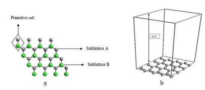
In past decade graphene has been widely explored for its novel properties. It is 2-Dimensional (2D) material exfoliated from layer of graphite with carbon atoms arrange in a honeycomb lattice with sp2 hybridization (Figure 1). The primitive hexagonal cell of graphene has two sub lattice A and B. Graphene has two simple edge geometries, first one is zigzag terminals involves only one sub lattice site and second is armchair terminal involves both sub lattices sites [2]. An individual carbon (C) atom has four bonds, one σ with each of neighbours C atoms and the other one is π-bond oriented out of plane. Inter-atomic distance of adjacent C atoms is 1.42 Å. σ bond in the 2D plane of this particular atomic configuration is a combination of s, px and py, whereas π- bond are composed of dangling out plane pz electron. [3]
This one atomic thinnest layer has very large surface area of approx. 3000 square meters per gram, with breaking strength of 42 N/m. Beside this it has high elasticity up to 20%. Graphene can be morphed into 0-D fullerenes, rolled into 1-D nanotubes or stacked into 3-D graphite. A pristine graphene layer has unique properties, zero band gap with a point-like Fermi surface [4]. The thermal conductivity of graphene is approximately 5000 Wm-1 K-1 (much larger than that of copper – 401 Wm-1 K-1). Due to massless relativistic charge carriers at Dirac point, high electrical conductivity (even greater than silver) at room temperature (ballistic transport), and high charge carrier mobility due to linear dispersion at the so-called Dirac point is observed. This 2D material conducts both heat and electricity better than any known material at room temperature. Graphene is a transparent material absorb only 2.3% of incident light, so can be used in graphene-based optoelectronic devices [5]. Due to its electronic, optical, thermal, magnetic, mechanical and electrochemical properties, graphene has attracted immense interest in diverse fields of research, such as electronics, optoelectronics, energy conversion and storage devices, water purification, prevent rusting of iron, lithium-ion battery, field effect transistor, gas sensors, and biomedicine. It is well seen that the zero band gap nature of graphene limits its application to device and optical purpose. Fortunately, this huddle can be overcome by engineering defect, functionalization and substitution on this monoatomic thin surface. In present work we focused on tuning the band gap of graphene by substituting C atoms on surface with Boron/Nitrogen atom. We have theoretically simulated graphene and its derivatives using density functional theory-based calculations [6].
Materials and Methods
Modelling details of grapheneWe started calculations by opting primitive cell of graphene having two types of sublattice A and B. The primitive cell consists of 2-atoms with bond-length of 1.42 nm. A 4 × 4 super cell is generated by periodic repletion of primitive cell along the x-y plane. To avoid periodic image interaction a large vacuum of 15 Å is considered along the z-axis, shown in Figure 1.
This atomic configuration is further optimized to ground state by using the density functional theory approach. The interaction between core and valence electrons of atoms are parameterized in terms of Trullier-Martien potential. Valence electrons are opted with a basis set of double-zeta polarized type. In Hamiltonian, exchange-correlation is chosen as Generalized Gradient Approximation (GGA) [8].
Result and Discussion
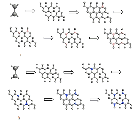
Boron/Nitrogen doped grapheneTo understand the effect of nitrogen and boron doping in graphene sheet, we constructed nitrogen and boron doped graphene sheet. Firstly, we build pristine graphene of 32-atom with periodical repetition of 2-atom unit cell in the x-y plane. After that fix the dimensions, replace one by one carbon atom with nitrogen and boron atom in two different graphene sheets. For every replacement carbon atom, we calculate the band structure and band gap of resulting doped sheet at every replacement atom. This method understood is increasing the dopant percentage by fixing the periodicity of graphene dimensions, as shown in Figure 2.
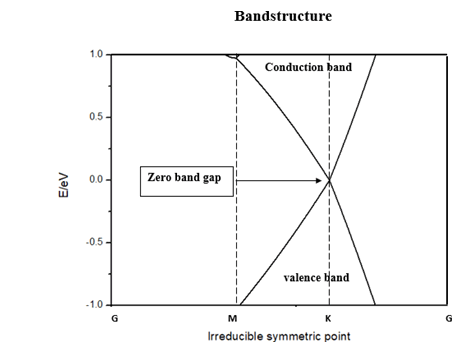
Before moving ahead to our objective first we checked the validity of computational method that we considered. To do it a primitive graphene unit is geometrically optimized followed by examining its band structure details. Thankfully, we get validated output with C-C bond length of 1.42 nm and zero-band gap at K of Brillouin zone (Figure 3). It is obvious from band structure diagram that the electronic charge carrier exhibit ballistic movement due to a drastic change in the gradient of the rate of change in energy [9].
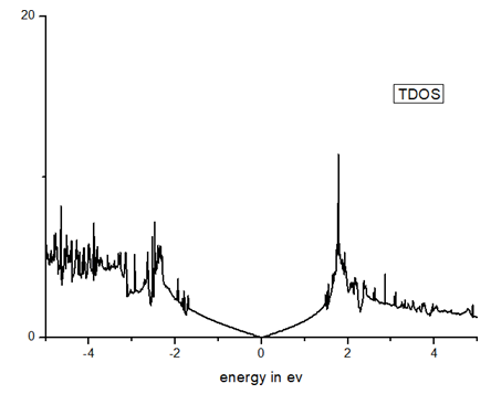
The density of state corresponding to band structure diagram is shown in Figure 4, the valence band regions are primarily consisting of valence pz orbitals or π type.
It is quite clear that zero band gap nature of graphene causes its limited application compared to semiconductors. Due to band gap, the latter are useful in device-application, opto-electronic purpose and so on, meanwhile apart of having appealing physical and chemical nature the former is almost untouchable for these purposes. To qualify a better status in device application and optical uses, band gap induction in graphene is required. From the literature survey, this can be achieved either by inducing defect or functionalization/substitution at the surface of this 2D material [10]. This work is focused on inducing band gap in graphene by substituting C atoms with B or N. Relative to C, boron is electron deficient and N is electron rich in nature. Substitution with these exotic atoms must consequence to change in electronic density of state that might play vital role in opening the band gap. With this intention, we have explored our rest of work in this thesis.
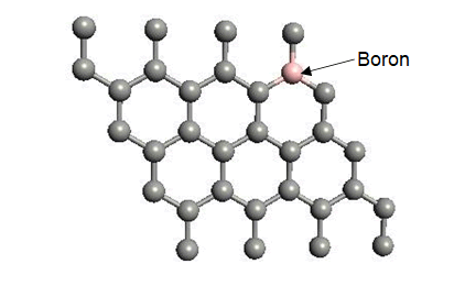
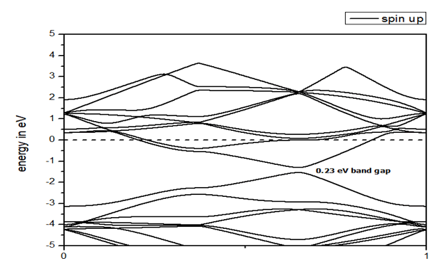
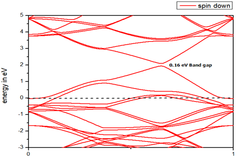
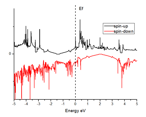
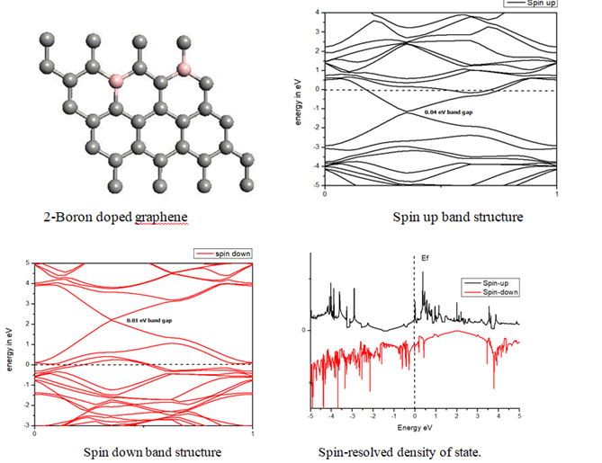
Boron substituted grapheneWhen we replaced a carbon atom from a boron atom, there is no significant distortion present in the 2D graphene structure because size of boron atom is approximately same and boron atom gave sp2 hybridization like carbon atom in graphene sheet. For this atomic configuration, the average measured B-C bond length is 1.48 Å, shown in Figure 5. There is small opening of 0.23 eV energy bandgap in spin-up shown in Figure 6 and 0.16 eV in spin-down (Figure 7) at K-point of Brillouin zone. Since B-toms are electron deficient nature and band structure diagram show shifting down of valence band maxima and valence band minima in spin-up and shifted upward in spin-down. Density of state plot as shown in Figure 8 exhibits asymmetric behavior across the Fermi level suggesting this material possess magnetic behavior.
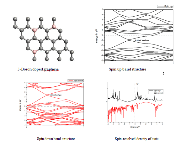
In density of state plot (Figure 8), material shows symmetric dispersion of spin up and down plot which signifies that material has a resultant spin magnetic moment, so it is used as magnetic material We further analysed the effect of multiple boron substitution over graphene sheet, i.e. percentage doping of 6%, 9%, and 12%. The calculated band gap and Fermi shift of these configurations are depicted in Table 1. However, an inconsistent trend in energy band gap of on increasing dopant percentage is observed (Figures 9-11).
| S. No. | Concentration of boron (%) | Band gap (eV) | Fermi level shifted downward (eV) | ||
|---|---|---|---|---|---|
| Spin up | Spin down | Spin up | Spin down | ||
| 1 | 3 | 0.23 | 0.16 | -1.39 | -2.82 |
| 2 | 6 | 0.04 | 0.01 | -1.17 | -2.23 |
| 3 | 9 | 0.22 | 0.15 | -0.91 | -2.42 |
| 4 | 12 | 0.17 | 0.1 | -0.64 | -2.63 |
Table 1: Boron doped graphene at different concentrations.
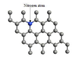
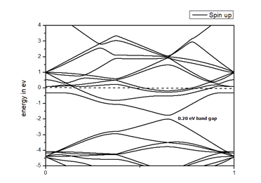
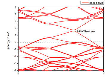
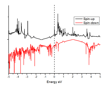
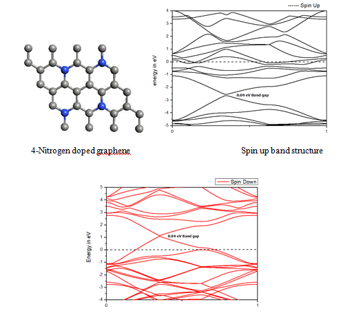
When we replaced a carbon atom from a nitrogen atom, there is no significant distortion present in the 2D graphene structure because size of boron atom is approximately same and boron atom gave sp2 hybridization like carbon atom in graphene sheet. For this atomic configuration the average measured N-C bond length is 1.37 Å, shown in Figure 12 There is small opening of 0.20 eV energy band gap in spin-up Figure 12 and 0.13 eV in spin-down Figure 13 at K- point of Brillouin zone. Since B-toms are electron deficient nature and band structure diagram show shifting down of valence band maxima and valence band minima in spin-up and shifted upward in spin-down. Density of state plot as shown in Figure 14 exhibits asymmetric behavior across the Fermi level suggesting this material possess magnetic behavior.
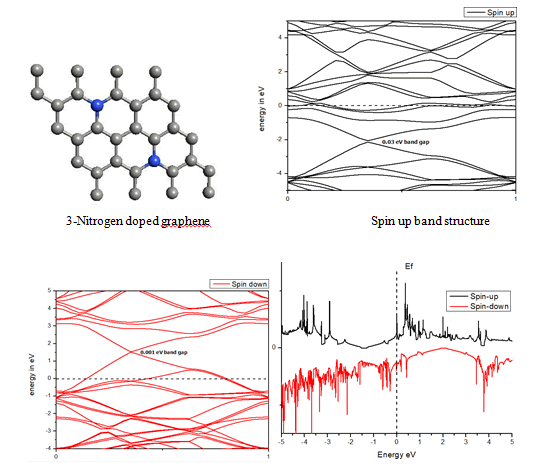
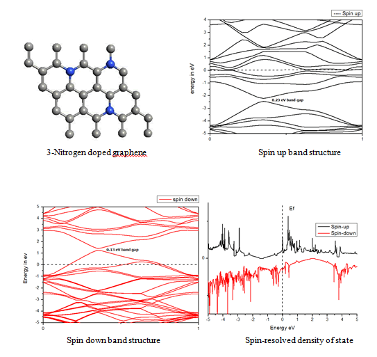
In density of state plot (Figure 15), material shows symmetric dispersion of spin up and down plot which signifies that material has a resultant spin magnetic moment, so it is used as magnetic material We further analysed the effect of multiple nitrogen substitution over graphene sheet, i.e. percentage doping of 6%, 9%, and 12%. The calculated band gap and Fermi shift of these configurations. However, an inconsistent trend in energy band gap of on increasing dopant percentage is observed (Figures 16-18) (Table 2).
| S. No. | Concentration of nitrogen (%) | Band gap (eV) | Fermi level shifted downward (eV) | ||
|---|---|---|---|---|---|
| Spin up | Spin down | Spin up | Spin down | ||
| 1 | 3 | 0.2 | 0.16 | -1.84 | 1.66 |
| 2 | 6 | 0.03 | 0.001 | -2.1 | 1.51 |
| 3 | 9 | 0.23 | 0.13 | -2.34 | 1.33 |
| 4 | 12 | 0.09 | 0.04 | -2.59 | 1.12 |
Table 2: Nitrogen doped graphene at different concentrations.
Conclusion
Boron and Nitrogen substituted graphene is explored in the present work. Literature survey and our DFT based calculations suggest pristine graphene as zero-band gap semiconductor. This electronic property limits their application for electronic device and optical purpose. To qualify it we introduced band gap by substituting B and N on this 2D nano surface. B and N substituted graphene introduced electronic band gap within range of 0.13-0.24 eV. Spin polarized DFT calculations suggest asymmetric DOS for spin up and spin down component. So, these materials also possess magnetic behavior. B and N substitutions are carried out at 3%, 6%, 9% and 12% concentration. Trend shows with increased doping concentration Fermi level decreased and increased, respectively, for B and N doped graphene. B-doped graphene serve as p-type semiconductor, meanwhile N-doped serve as n-type semiconductor.
References
- Holyst R (1991) Landau-Peierls instability x-ray diffraction patterns and surface freezing in thin smectic films. Phys Rev 44: 3692.
- Pooja Rani, Jindal VK (2012) Designing band gap of graphene by B and N dopantatoms. RSC Adv 3: 802-812.
[Crossref][Google Scholar][Indexing At]
- Nigar S, Zhou Z, Wang H, Imtiaz M (2017) Modulating the electronicand magnetic propertiesof graphene. RSC Adv 7: 514546-51580.
- Boehm HP, Clauss A, Fischer GO, Hofmann U (1962) "Das Adsorptionsverhalten sehr dünner Kohlenstoff-Folien". Zeit für Anorg Allg Chemie 316: 3-4.
- Wei DC, Liu YQ, Wang Y, Zhang HL, Huang LP, et al. (2009) Synthesis of N-doped graphene by chemical vapor deposition and its electrical properties. Nano Lett 9: 1752-1758.
- Castro AH, Guinea F, Peres NMR, Novoselov KS, Geim AK, et al. (2009) The electronic properties of graphene. Rev Modern Phys 81: 109-162.
- Yang XB, Liu GX, Balandin AA, Mohanram K (2010) Triple-mode singletransistor graphene amplifier and its applications. ACS Nano 4: 532-553.
- Huang B, Yan QM, Zhou G, Wu J, Gu BL, et al. (2007) Making a field effect transistor on a single graphene nanoribbon by selective doping. App Phy Lett 91: 4-9.
- Romero HE, Joshi P, Gupta AK, Gutierrez HR, Cole MW, et al. (2009) Adsorption of ammonia on graphene. Nanotechnology 20: 3-4.
- Bonaccorso F, Sun Z, Hasan T, Ferrari AC (2010) Graphene photonics and optoelectronics. Nature Photonics 4: 611-622.
 Spanish
  Chinese
  Russian
  German
  French
  Japanese
  Portuguese
  Hindi
Hindi 