Spanish
  Chinese
  Russian
  German
  French
  Japanese
  Portuguese
  Hindi
Hindi Research Article, J Electr Eng Electron Technol Vol: 6 Issue: 2
Biasing LDMOS Amplifiers Employing a Simple Passive Temperature to Voltage Converter
Antonis Constantinides*
Kononos 31, 3087, Limasso, Cyprus
*Corresponding Author : Antonis Constantinides
Kononos 31, 3087, Limasso, Cyprus
Tel: +35799571857
E-mail: etbroadcast@gmail.com
Received: June 16, 2017 Accepted: July 07, 2017 Published: July 14, 2017
Citation: Constantinides A (2017) Biasing LDMOS Amplifiers Employing a Simple Passive Temperature to Voltage Converter. J Electr Eng Electron Technol 6:2. doi: 10.4172/2325-9833.1000142
Abstract
This paper presents the quiescent current’s (IDQ) variations over temperature and a simple method of compensation concerning a laterally diffused Metal-Oxide-Semiconductor (LDMOS) amplifier. It has been justified in real condition measurements that quiescent current is progressively increasing proportionally to temperature variations of the LDMOS causing instability to the parameters of the amplifier. In order to be compensated over a wide range of temperature variations, e.g. 40-80 degrees Celsius, a very simple Temperature to Voltage converter (sensor) has been developed. This sensor can also be applied on any other MOSFET amplifier that its quiescent current is drifting proportionally to temperature variations as well. That is, the mentioned sensor has been installed in many different amplifier units employing various types of LDMOSs and it has been operating as expected. Since it is very simple to be simulated and constructed, it is recommended to be demonstrated to the scientific society which conducts research in this area.
Keywords: LDMOS; Amplifiers; Temperature variations; Quiescent current;Therapeutic ultrasounds; Medical equipment
Introduction
LDMOS semiconductors are currently used by almost all commercial RF amplifiers today [1,2] but can also be applied in applications such as therapeutic ultrasounds and in other medical equipment. The reason is because LDMOS provide high gain, high power output and very good operating reliability [3]. As a result, a single LDMOS device eliminates complex circuits that consist of many switching FET’s as in traditional amplifiers manufactured for the High Frequency bands (HF). As far as the above mentioned parameters are concerned, they are considered very important for the specifications and the long run reliability of a signal amplifier and must be kept constant under any operating conditions [4]. For example, an important parameter that can affect the above is the temperature that develops on the LDMOS case and spreads on the heat sink where the effects are listed below. The quiescent current is a very important factor that determines the final performance of an LDMOS amplifier [5]. It has been justified experimentally that the quiescent current is progressively increased depending on the temperature of the semiconductor even when the amplifier is not driven [6]. It occurs when it exceeds 0.7A as shown in Figure 1. The temperature versus IDQ is also expressed by Eq.1.

Figure 1: Quiescent current is progressively increased over a wide range of temperatures.
IDQ=0.0308*T+0.6781 (1)
Where:
IDQ=Quiescent Current
T=Temperature in Celsius
One very good way to stabilize the quiescent current has been recommended by free scale [4]. It is achieved by the use of a small transistor (Q1) in the bias circuitry as a thermal tracking device that is presented in Figure 2. The disadvantage of the above mentioned is that much experimentation is needed with various low power BJT devices in order to detect the right device that has a temperature coefficient identical to the one of the LDMOS at specific quiescent current value. It is also worth noting that different quiescent current ratings have different slopes and different temperature coefficients. Similar techniques employing active devices of biasing LDMOS have been also demonstrated in various experiments [1,5-8].
Figure 2: The bipolar NPN transistor (Q1) is used as a thermal tracking device.
Alternatively, after many laboratory tests and mathematical simulations a very simple but precision passive circuit has been developed that can be applied on all LDMOS amplifiers with very good results as follows. This circuit’s innovation is that it is very simple, can be constructed with the same materials every time for every temperature coefficient and quiescent current rating as analysed below:
The circuit is a simple sensor that can precisely detect the temperature on the semiconductor’s die and be self-adjusted so that the quiescent current is kept constant in a wide range of temperatures such as between 40-80°C.
Materials and Methods
The first step towards the development of the sensor was to investigate the behaviour of the LDMOS in various temperature ratings relative to the quiescent current. The quiescent current is determined by the voltage at the gates of the LDMOS (VGS). The temperature was measured on the die of the LDMOS. For this research, a well-known semiconductor LDMOS MRFE6VP61K25H was adapted because it is used by many manufacturers in power amplifiers ranging of 1KW CW (Po=1200 W 1.8-600 MHz). The MRFE6VP61K25H may also operate at lower frequencies e.g. 0.5MHz but providing less output power and will be discussed in another paper (Table 1).
| BIAS | Die Temp | IDQ(A) | ΔV (mV) |
|---|---|---|---|
| 2.62 | 40 | 2.3 | 30 |
| 2.59 | 50 | 2.3 | 20 |
| 2.57 | 60 | 2.3 | 20 |
| 2.55 | 70 | 2.3 | 30 |
| 2.52 | 80 | 2.3 | Average: 25 |
Table 1: The variation of VGS so that the IDQ is constant at 2.3 A which is calculated at 2.5 mV/C.
Figure 3 presents the variation of VGS in terms of temperature developed on the semiconductor’s die when IDQ= 2.3A. It is also expressed by equation 2 below:

Figure 3: VGS versus temperature to keep IDQ constant.
T=3860V2-20320V+26785 (2)
Where:
T=LDMOS die Temperature
V=VGS (Gate source voltage)
Knowing all parameters that concern the temperature in terms of VGS the sensor has been based on the following principles. For the mentioned circuit’s development, the temperature on the LDMOS die must be detected at any time with precision. For this purpose a 47K thermistor was used where the characteristics are given in Figure 4.

Figure 4: Temperature versus resistance of the 47K thermistor.
The change of temperature on the LDMOS’s die relative to the resistance of the thermistor is also given by Figure 4 where equations 3 and 4 have been derived as they are given below:
T=1E-07R2-0.0059R+110 (3)
R(ΚΩ)=8,2T2-1449T+68657 (4)
Where:
T=Temperature in degrees Celsius
R=Resistance in Ohms
Results
The sensor is presented in Figure 5. It consists of a resistor network and the thermistor that works as a thermal tracking device. The thermistor must be installed on the die of the LDMOS in order to guarantee a very good contact with the true temperature’s enhancement. In this respect, the final equation that determines the compensated Vbias in terms of the temperature change on the die of the LDMOS is expressed in Eq.5 below

Figure 5: The temperature to voltage compensation circuit.
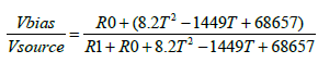 (5)
(5)
In order to determine the unknown resistors R1 and R0 for a specific temperature coefficient rating, it can be achieved by solving the system of two equations two unknowns (Equations 6-7):
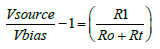 (6)
(6)
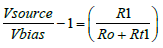 (7)
(7)
Where:
V-source: The voltage of the source, e.g. 5 V
V-bias: The VGS that determines the desired quiescent current at 4°C
V-bias1: The VGS at 5°C that compensates the drift of quiescent current
R1=Unknown Resistor
R0=Unknown variable resistor
Rt=the resistance of the 47K thermistor at 4°C (from data sheet)
Rt1=the resistance of the 47K thermistor at 5°C (from data sheet)
As an example, for a temperature coefficient of approximately -2.5 mV/C, Source=5 V, R1=219K and R0=220K. The data of the simulation are given in Table 2 below. The data (Bias Specs) in the first column have been gathered from the LDMOS data sheet. The data of the second column (compensation) represent the actual bias compensation of the sensor. The use of the variable resistor R0 is for the fine adjustment of quiescent current’s drifting.
| BIAS Specs | Compensation | Die Temp Celsius | IDQ(A) |
|---|---|---|---|
| 2.62 | 2.6291 | 40 | 2.3 |
| 2.59 | 2.5921 | 50 | 2.3 |
| 2.57 | 2.5663 | 60 | 2.3 |
| 2.55 | 2.548 | 70 | 2.3 |
| 2.52 | 2.5345 | 80 | 2.3 |
Table 2: The actual versus the theoretical value of VGS so that the IDQ is constant at 2.3 A which is calculated at 2.5 mV/C.
The compensated IDQ between 40-80°C is presented in Figure 6.

Figure 6: Temperature versus IDQ after compensation.
Conclusion
This paper has presented a very simple passive Temperature to Voltage converter that operates as a sensor for biasing LDMOS amplifiers. Because it is very simple, it eliminates the need of adaptive complicated active device circuitries which have been discussed by other authors presented in this document. Another crucial key point of this network is that it can be simulated very easily in order to operate for any temperature coefficient and quiescent current ratings by solving a simple system of equations. Therefore, it is very useful for biasing LDMOS amplifiers operating in Class A and AB, with very good results avoiding complicate procedures and experimentation.
References
- Constantinides A, Christos Y, Christakis D (2014) Improving the LDMOS temperature compensation bias circuit to optimize back-off. International Journal of Electrical, Computer, Energetic, Electronic and Communication Engineering 8: 1104-1106.
- Tan Y, Kumar M, Sin JKO, Cai J, Lau J (2000) A LDMOS technology compatible with CMOS and passive components for integrated RF power amplifiers. IEEE Electron Device Lett 21: 82-84.
- Heijden VD, Mark P (2002) Theory and design of an ultra-linear square-law approximated LDMOS power amplifier in class-AB operation. IEEE Trans Microw Theory Techn 50: 2176-2184.
- http://pdf.datasheetcatalog.com/datasheet/motorola/MRF175LV.pdf
- Duclercq J, Olivier L (1998) LDMOS Power Modules for GSM Base Station Application: Optimum Biasing Circuit. Freescale Semiconductor Application Note ΑΝ1643.
- Blair C (2000) Biasing LDMOS FETs for linear operation. Applied Microwave and Wireless 12: 90-94.
- Johansson J (2001) Gate biasing arrangement to temperature compensates a quiescent current of a power transistor. U.S. Patent No. 6,288,596, USA.
- Theeuwen SJCH, Qureshi JH (2012) LDMOS technology for RF power amplifiers. IEEE Trans Microw Theory Techn 60: 1755-1763.