Spanish
  Chinese
  Russian
  German
  French
  Japanese
  Portuguese
  Hindi
Hindi Research Article, J Electr Eng Electron Technol Vol: 14 Issue: 3
Comparative Analysis of Current Starved VCO with Sleep Stack Approach for PLL Applications
Kalaka Annamma1*, Sobhit Saxena1 and Govind Singh Patel2
1Department of Electrical and Electronics Engineering, Lovely Professional University, Phagwara, India
2Department of Electronics and Communication Engineering, Sharad Institute of Technology, Ichalkaranji, India
*Corresponding Author: Kalaka Annamma
Department of Electrical and Electronics Engineering, Lovely Professional University, Phagwara, India
E-mail: anusasmi@gmail.com
Received: 02-Dec-2024, Manuscript No. JEEET-25-153853; Editor assigned: 05-Dec-2024, PreQC No. JEEET-25-153853 (PQ); Reviewed: 19-Dec-2024, QC No. JEEET-25-153853; Revised: 07-Aug-2025, Manuscript No. JEEET-25-153853 (R); Published: 14-Aug-2025, DOI: 10.4172/2325-9833.1001027
Citation: Annamma K, Saxena S, Patel GS (2025) Comparative Analysis of Current Starved VCO with Sleep Stack Approach for PLL Applications. J Electr Eng Electron Technol 14:3.
Abstract
This study compares the performance of the Current Starved Voltage Controlled Oscillator (CSVCO) for Phase Locked Loop (PLL) solutions. To complete the current job or the design of the Current Starved VCO, the sleep stack reduced power leakage technique is used. With a 0.45V supply voltage and 45 nm CMOS technology, it has been implemented using Cadence Software. Characteristics including latency, oscillation frequency and average power are calculated. The improved cadence simulation performance results are recorded. The proposed PLL implementation parameters with sleep stack are confirmed to be significantly smaller on a chip than earlier approaches. While using a lot less electricity and far more efficiency. This is verified by contrasting the different PLL implementation parameters using Basic CSVCO and Sleep Stack CSVCO. For low-power applications, the sleep stack method works best. The proposed PLL architecture employing the sleep stack technique successfully lowers sub-threshold leakage current. A frequency of 2.759 GHz, power of 2.559 μw, phase noise of -63.8 (dBc/Hz) and latency (μs) of 0.0006544 are also attained.
Keywords: Control voltage; Gain; Gale-or; Lector; Sleep stack; Tuning range
Introduction
The Phase Locked Loop (PLL) control mechanism is utilized to ascertain the relationship between the phase of the input and output signals. Oscillator with phase detector with voltage control-within the feedback loop, the two primary components are oscillators and phase detectors. One of the key blocks, VCO, is included in this research. V Cos are used in communication systems for their basic functions.
Because of their high frequency, low noise, wide tuning range and area occupancy, ring oscillators and LC oscillators are significant among the several types of V Cos. The LC VCO takes up more room because it is composed of an inductor and a capacitor. Although they take up more room, the delay cells that comprise the ring oscillators function similarly to the buffer. In a ring oscillator, feedback happens when the input of the first delay cell is connected to the output of the last delay cell. Differential or single-ended delay cells may be used, depending on the circumstances [1].
As the number of delay cells increases, the area will be used up. Variations in driving capability cause its features to behave nonlinearly; this can be prevented by using a feedback circuit. This adds an additional stage to the circuit, increasing its cost. In order to address the limitations of its predecessors, the prior VCOs, the current starves VCO strategy was developed. This document is organized as follows. Section 2 describes the basic Current Starved VCO. Section 3 discusses various techniques for lowering leakage power in CMOS devices. In Section 4, simulation results and design comparisons are displayed. Section 5 marks the final conclusion of this study [2].
The current work for CS sleep VCO was created using CMOS 90 nm technology, which operates at a frequency of 1 GHz with a tuning range of 1-5.8 GHz and a power dissipation of 8.12 μW. Low power leakage strategies that can be used with 45 nm technology include stacking, galeor, lector and MTCMOS. The existing CSVCO has drawbacks compared to 180 nm, 90 nm and 65 nm CMOS technology in terms of power consumption, delay, area and signal quality [3].
Traditional stacking methods, such as sleep stacks and dual sleep stacks, have faster leakage currents because of the supply voltage. Three transistors are positioned to prevent this, increasing the area penalty. To further reduce power consumption, the Sleep stack technique will be used to design and implement CSVCO in 45 nm CMOS technology. It will be compared to various low leakage power strategies.
Design and analysis of a phase locked loop sleep voltage controlled oscillator with low power and high frequency current starvation-this study proposes several inverter delay techniques, including stack delay cell, sleepy stack delay cell and sleep delay cell in current starved VCO, to minimize leakage power. A decrease in the leakage current below the threshold the sleeping transistor in an inverter, the sleep transistor is placed between the pull-up MOSFET and the supply voltage, producing a reverse bias and producing a result when both are off. The CSVCO is designed using 90 nm CMOS technology [4].
Previous research was compared with the proposed present insufficient VCOs. The older method uses a lot of power but has a good oscillation frequency, a small tuning range and less area. It is becoming less and less appropriate for the latest high-speed courses. The hungry VCO stack, also referred to as the recommended drowsy stack, outperforms previous iterations. The design and implementation of high speed and low power PLLs Sridhar et al., discuss the use of GPDK 45 nm technology. In this work, an efficient PLL that employs a current-starved voltage-controlled oscillator is meant to maintain the linearity of the gain. The results show that the optimized PLL has excellent stability and noise immunity, with a locking range of 63.16 Hz, a pull-out range of 0.75 s and a locking time of 43.82 Hz.
The design and analysis of seven-stage MOS current mode logic power gated MOSFETs can be effectively demonstrated by using a current-starved voltage-controlled oscillator for the phase-locked loop application. Output noise, tuning range, phase noise, oscillation frequency and average power are among the parameters.
Madheswaran and Panneerselvam assert that the Monte-Carlo analysis produces better results [5].
This existing work, which covers the scope of using this CSVCO with a low power leakage methodological method to provide improved values of performance parameters, is used by applications in the Sivasakthi and Radhika in 2024 used the bulk driven keeper technique at 45 nm CMOS technology to construct and analyze a PVT-tolerant hybrid current-starved ring VCO for the PLL application.
The recommended architecture is perfect for PLL applications including wireless and radio frequency communication and performs better than earlier designs in a number of performance criteria. By employing transistors with pull-up and pull-down sleepy stacks, the oscillation frequency is increased by 80.18 percent. Better its phase noise and FOM improvements are 19.29% and 13.74%, respectively, while its frequency tuning range is 59.39%. After a difficult literary after a comprehensive review of the literature, it was concluded that further study is needed to improve the performance of the VCO by examining a few features, such as noise, low leakage power, wide tuning frequency range and delay [6].
Materials and Methods
Previous studies are compared with the proposed current starved VCOs (CS Sleep VCO). The previous work generates a respectable oscillation frequency, but because of its low tuning range, low area and high power consumption, it is more inappropriate for the latest high-speed circuits. The proposed current deprived VCO (stack, sleep, fatigued stack) performs better than the previous experiments. A high frequency, a broad tuning range and fewer VCO comparisons of several parameters are the main features of the proposed currentdeprived sleep VCO. The proposed CS sleep VCO has a frequency of 11.3 MHz, a wide tuning range of 1-5.8 GHz and a reduced power dissipation of 0.0427 pW than previous designs [7].
Full-swing output is provided by the CS sleep VCO without the need for an output stage buffer. The main advantages of the aforementioned VCO are its wide tuning range, low power dissipation and high oscillation frequency. The threshold voltage for the MOSFET's OFF condition increased in the suggested delay cell strategies. The CSVCO uses delay cell techniques, and the CSVCO that uses sleep delay cells achieves low power consumption and a broad tuning range. The CS Sleep VCO is made using 45 nm CMOS technology with a 0.3 V power supply. With a power dissipation of 0.0427 pW, the device achieves a broad tuning range between 1 and 5.85 GHz with phase noise of -115 dBc/Hz at 11.3 MHz (Figure 1).
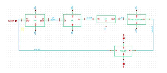
Figure 1: PLL architecture with sleep stack CSVCO.
The two primary parts of the PLL are a voltage-controlled oscillator and a phase detector in a feedback loop. One of the main blocks that is demonstrated in this study is VCO. The main tasks of the VCOs are carried out by the communication systems. Among the several types of VCOs, ring oscillators and LC oscillators are essential due to their high frequency, low noise, wide tuning range and area occupancy. The LC VCO requires more room because it is composed of an inductor and a capacitor. The simulation findings show that the CS Sleep VCObased PLL is sufficient to satisfy the clock generation reliability requirements of high-speed networks. Phase Locked Loops (PLLs) are control systems that generate an output signal whose phase is associated with the input signal's phase [8].
The ring oscillators' delay cells function similarly to the buffer but require more room. In a ring oscillator, the output of the final delay cell is fed into the input of the initial delay cells. This is known as feedback. The inverter delay unit can be used with a sleep, stack or sleep stack inverter to reduce the leakage power. As a result, the delay cells are either single-ended or differential. In all cases, time and behavior can be controlled with Vctrl. An increase in the number of delay cells leads to the consumption of area. By including a feedback circuit, the VCO's characteristics are kept from becoming nonlinear as a result of changes in driving capability.
The inclusion of this feedback circuit raises the circuit's cost even further. The current starved VCO technique was developed to overcome the shortcomings of the previous VCOs. This previous study focused on optimizing the leakage power to improve PLL performance using a variety of low-power reduction approaches. This study uses a revolutionary low-power PLL design that introduces the sleep stack technique based on the current starved ring VCO to demonstrate a wide tuning range, reduced phase noise, reduced area and reduced delay. The analysis was plotted at different temperatures and at multiple process corners. It is widely applicable to PLL applications. The proposed current starved ring-based VCO with sleep stack technique reduces phase noise, power and latency.
In order to address the sub-threshold leakage power in the suggested circuit, the sleep stack technique has been employed in the CSVCO circuit, both above and below the pull up and pull down networks, respectively. The stack transistors would reduce leaks once the sleep transistor entered sleep mode in normal mode. When the sleep transistor is turned on and the stack transistors are turned off, the CSVCO circuit's leaks are reduced in the active state.
Sleep stack approach for current starved VCO
The stack approach is used to build the CSVCO circuit. The sleep and stack techniques are applied above and below the pull-up and pull-down networks, respectively. The sleep transistor would go into sleep mode in normal mode and the stack transistors would then minimize leaks. The CSVCO circuit's leaks are minimized by turning the sleep transistor on and the stack transistors off in the active state. The sleep stack method is especially helpful when power efficiency is a key design consideration or in low-power applications, as it helps to reduce power consumption without sacrificing the circuit's speed or functionality [9].
The alternate configuration of the proposed circuit aims to reduce the number of transistors and as a result, the area consumption. Because of the alternative arrangement of the suggested design itself, the circuit works more efficiently to reduce sub-threshold leakage current, which lowers power consumption. Therefore, the sleepy stack technique does not have to be used to connect all of the delay cells in the proposed design.
Current-starved voltage-controlled oscillator sleep stack approach for designing phase-locked loop architecture
Examining the root causes of malfunctions or performance problems is known as "analysis of cause" in wireless network technology. It looks at things like network congestion, hardware issues and signal interference that might affect efficiency and connectivity. Solutions to improve dependability and maximize network performance can be created by investigating these issues (Figure 2).
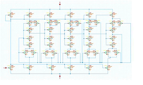
Figure 2: Sleepy stack technique for the current starved VCO the circuit.
When it comes to frequency and driving power, ring oscillators outperform the other types of VCOs. In the design of the ring VCO, there is a delay stage. With an increase in these delay stages, the circuit becomes nonlinear. Although this non linearity can be handled by increasing the number of delay cells, doing so raises the circuit's complexity and power consumption. Unlike a current-starved VCO, which controls the current, a basic VCO controls the output frequencies using the control voltage. Delay cells make up the circuit and a current mirror regulates the amount of current that goes to each delay cell.
Power usage and leakage have increased as a result of the present demanding VCO. Low leakage techniques on the delay cells and a change in the aspect ratio of the transistors, which reduces the threshold voltage, can further reduce these leakages. Performance can be analyzed using a number of parameters, including average power, frequency and latency. The Sleep Stack technique was utilized in this work to create the CSVCO with the least amount of power loss. It was also applied in PLL for Higher Stability, which computed numerous parameters. Contrasted as well with the conventional and recommended methods.
Results and Discussion
Outcome and conversations
The circuit has been created in the virtuoso tool in Cadence Software in 45 nm technology with a supply voltage of 0.45 V in order to evaluate the circuit and carry out the simulation result of the CSVCO implemented various low leakage strategies. By initializing the output node to either 1 or 0 to produce the required oscillations, the oscillator's simulated output is obtained. Consideration is given to room temperature (27°C) and a control voltage of 0.45 V in order to compute characteristics like gain, average power (Pavg), delay and oscillation frequency (Figure 3 and Table 1).
| S. no. | Leakage power methods | Average power (W) | Area (μm2) | The delay (μs) | Frequency (GHz) | Gain in Ghz/V | Tuning range in (%) |
| 1 | Gale-or | 48.21 e-9 | 37.5768 | 19.57 | 13.8 | 3.07 | 56.22 |
| 2 | Lector | 49.76 e-9 | 35.58122 | 32.24 | 14.33 | 3.19 | 6.071 |
| 3 | Sleep | 40.46 e-12 | 26.3168 | 327.81 | 72.12 | 16.02 | 98.75 |
| 4 | Stack | 49.57 e-9 | 56.4002 | 19.03 | 30.46 | 6.76 | 14.72 |
| 5 | Sleep stack | 58.33 e-9 | 37.5768 | 0.4895 | 58.87 | 13.87 | 34.85 |
Table 1: Simulation outcomes for CSVCO parameters using various low leakage power strategies.
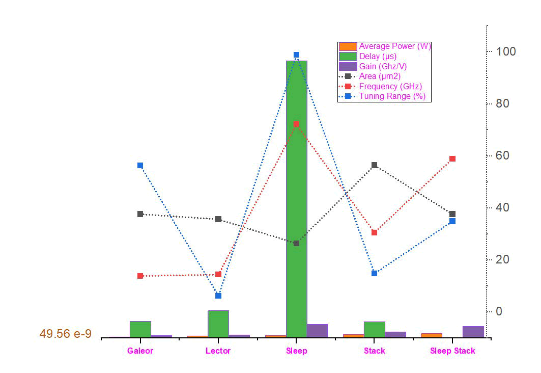
Figure 3: CSVCO parameter analysis using a variety of low leakage power techniques.
Setups PLL using basic CSVCO and SLEEP STACK CSVCO VCO type with 45 nm technology is the recommended task (Table 2).
| Parameters | PLL with basic CSVCO | Proposed work-PLL with Sleep Stack CSVCO |
| VCO type | Ring | Ring |
| Tech (NM) | 45 | 45 |
| Freq (GHz) | 2.592 | 2.769 |
| Supply volt (v) | 1 | 1 |
| Power (MW) | 0.002787 | 0.002455 |
| P-Noise (dBc/Hz) | -72.21 | -63.72 |
| Delay (µs) | 0.866 | 0.000654 |
Table 2: Sleep stack versus PLL CSVCO the PLL CSVCO comparative analysis.
According to the simulation results of parameter analysis using low leakage power approaches and the above table, the current starved VCO with sleep stack and keeper methodology is intended to address the issues with the current VCO in high frequency, wide tuning applications. Phase noise, leakage power and a narrow frequency range are further difficulties. In order to guarantee its resilience, comprehensive simulations are conducted in harsh environments, including various process corners, fluctuating control voltage and extremely high or low temperatures. Power consumption is lower in the suggested CSVCO PLL circuit. Due to the pull-down and pull-up sleeping stacks transistor arrangement, resulting in a 20% increase in oscillation frequency. Additionally, the frequency tuning range is improved by 27% using the proposed circuit. Furthermore, it lowers FOM growth by 10.74% and phase noise delay by 17.29%, respectively.
The above figure demonstrates the suggested design's robustness, making it a good choice for high-frequency applications. A supply voltage increase of 1 V is achieved. To ascertain the stability of the circuit, Monte-Carlo analysis is also carried out for a variety of parameters. According to the findings, the recommended design is optimal for PLL applications like wireless and radio frequency communication and outperforms earlier designs in a variety of performance criteria (Figure 4).
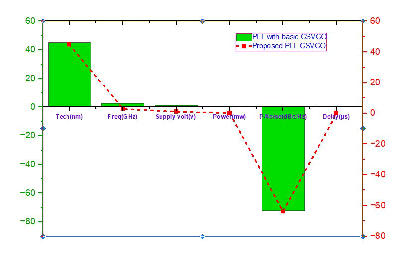
Figure 4: PLL CSVCO and Sleep Stack PLL CSVCO comparison analysis.
Conclusion
The Sleep Stack approach is a promising solution for improving the efficacy of CSVCOs for PLL applications. The oscillator's working mode can be dynamically changed to save a substantial amount of power without sacrificing functionality. The Sleep Stack CSVCO can be made even more effective and efficient by using the optimization strategies described in this work.
The tabular column above and the plotted graphs show that any low leakage power strategy utilized with the present CSVCO is superior in one or more aspects, including average power, oscillation frequency, delay and gain. From corner analysis, the power and delay also climb with increasing temperature from 27°C to 80°C and fall with decreasing temperature. When the temperature drops to -40°C.
When comparing Sleep Stack CSVCO and Basic CSVCO with the various PLL implementation parameters, it is discovered that Sleep Stack performs better. Change the CSVCO's supply voltage and stage count from 5 to 7, 9, 11, and so on. You may also increase other parameters like area and power to reach even higher frequencies.
Information on Funding
Inapplicable.
Assertive
The Central Institute of Tool Design in Hyderabad's Department of Electronics and Communication Engineering is acknowledged by the authors for providing the resources (EDA Lab-Cadence Virtuoso tool) for this investigation.
Interest Conflicts
The writers claim that there is no conflict of interest.
References
- Azadmousavi T, Ghafar-Zadeh E (2023) Design and analysis of a low-voltage VCO: Reliability and variability performance. Micromachines 14: 2118.
[Crossref] [Google Scholar] [PubMed]
- Madheswaran S, Panneerselvam R (2024) Design and analysis of 7-stage MOS current mode logic power gated MOSFETs in current starved voltage-controlled oscillator for the phase locked loop application. Int J Elec Comp Eng 14.
- Sivasakthi M, Radhika P (2024) Design and analysis of PVT tolerant hybrid current starved ring VCO with bulk driven keeper technique at 45 nm CMOS technology for the PLL application. AEU-Int J Elec Comm 173: 154987.
- Pothina CK, Singh NP, Prasanna JL, Santhosh C, Kumar MR (2023) Design of efficient phase locked loop for low power applications. Eng Proc 34: 14.
- Singh B, Kumar S, Chauhan RK (2023) Design of energy efficient VCO for PLL application. Analog Integr Circuts Signal Process 114: 31-40.
- Ellaithy DM (2023) Voltage-controlled oscillator based analog-to-digital converter in 130-nm CMOS for biomedical applications. J Electr Syst Inf Technol 10: 38.
- Gurjar R, Mishra DK (2023) Design and performance analysis of low phase noise LC-voltage controlled oscillator. Telecomm Comp Elect Cont 21: 872-880.
- Ellaithy DM (2023) Voltage-controlled oscillator based analog-to-digital converter in 130-nm CMOS for biomedical applications. J Electr Syst Inf Technol 10: 38.
- Pothina CK, Singh NP, Prasanna JL, Santhosh C, Kumar MR (2023) Design of efficient phase locked loop for low power applications. Eng Proc 34: 14.