Spanish
  Chinese
  Russian
  German
  French
  Japanese
  Portuguese
  Hindi
Hindi Research Article, Res J Opt Photonics Vol: 2 Issue: 2
Design of Nonlinear Kerr Lens (NKL) and Method of Implementation of All Optical Logic Gates and Processors using a Single NKL
Mukherjee K* and Raja A
Physics Department, B.B. College, Asansol, West Bengal 713303, India
*Corresponding Author : Mukherjee Kousik
Physics Department, B.B. College, Asansol, West Bengal 713303, India
Tel: 09434122481
E-mail: lipton007@rediffmail.com
Received: April 02, 2018 Accepted: April 03, 2018 Published: April 10, 2018
Citation: Mukherjee K, Raja A (2018) Design of Nonlinear Kerr Lens (NKL) and Method of Implementation of All Optical Logic Gates and Processors using a Single NKL. Res J Opt Photonics 2:2.
Abstract
A design of nonlinear lens using Kerr effect is described. The incident light changes the focal length of the lens and this light induced focal length change are utilized to optical switching and routing. Using this type of lens all optical 3 input AND, X-OR and majority function logic gates, two input AND, X-OR, NAND, NOR, X-NOR, optical processors half Adder, Full Adder are implemented. Controlled operation of the logic gates is also explained.
Keywords: Kerr effect; Optical switching; Optical logic gate; Optical logic processors
Introduction
Optics has established itself as a promising candidate for future parallel computation and communication system. All optical switching has an important role for implementation of the optical computation and communication system components. There are several types of switching techniques based on different kind of optical phenomena and materials. Nonlinear material based switching is very important for the application in optical switching technology. Different nonlinear phenomena in Semiconductor optical amplifier (SOA) [1], periodically poled lithium niobate (PPLN) [2], high nonlinear fiber (HNLF) [3], difference frequency generation (DFG) [4], Second harmonic generation (SHG) with optical parametric amplification (OPA) [5], nonlinear prism based on refraction [6], total internal reflection prism [7-9], nonlinear-linear slab (NL-L) [10,11], etc are utilized to design optical logic gates and processors by various researchers. SOA based devices require proper biasing current for its operation, PPLN has the disadvantages of having temperature and polarization sensitiveness, DFG and parametric process are very difficult to be implemented and requires high power lasers. The HNLF require a large length to show considerable effect, otherwise very popular nonlinear device and total reflectional prisms require high power for its operation. In contrast, nonlinear prism and NL-L slab based devices are very effective having no such drawbacks [6,10,11], which are based on optical Kerr effect. The effectiveness of the switching depends on the amount of deviations produced by the nonlinearity of the devices (materials) and is better for prism shaped devices compared to slab structure [6] and devices based on absorption are less susceptible to optical damage and has less speed of operation compared to refraction based devices which will be proposed in this communication. However, the deviation produced by a prism depends on the angle of incidence, and very small deviations can be produced for high intensity. Comparatively a lens can produce more deviation with same intensity and its focal length does not depend on the angle of incidence but is a constant quantity for a particular lens material and surroundings. It depends on the radii of curvature of the curved surfaces and can be adjusted to make the focal lengths as desired. In this communication a nonlinear lens utilizing Kerr effect in nonlinear materials. The variation of focal length, variation of Change of focal length, angular deviation corresponding to focal length with intensity of the incident light is analyzed. The all-optical switching based on the NKL is utilized to design logic gates and processors like three input AND, X-OR and majority function logic gates, two input AND, X-OR, NAND, NOR, X-NOR, optical half Adder, full Adder. The devices based on NKL are cascade-able, and higher order logic processors can be implemented using this in future.
Theory of Optical Switching and Design of Nonlinear Kerr Lens (NKL)
The refractive index of many optical materials depends on the intensity of the light, and is called Kerr effect, by analogy with the traditional Kerr electro optic effect. This effect can be explained by nonlinear polarization and the intensity dependent refractive index is given by
 (1)
(1)
Here ‘I’ represents the intensity of the incident light, n0 represents the usual weak field refractive index, and n2 is the nonlinear correction term. The nonlinear change may be produced by several mechanisms such as electronic polarization, molecular orientation change, thermal effects, photo-refraction etc. Electronic polarization produces n2 with response time of femto-seconds and thus very fast.
This refractive index change is utilized to change direction of propagation of a light beam of suitable intensity and optical switching can be achieved. In a nonlinear medium, this refractive index change produces several effects like self focusing, self trapping, phase conjugation, optical bi-stability etc may be useful for optical logic processors and memory devices. Few important nonlinear materials with values of linear and nonlinear refractive indices are listed in. Table 1 shows that some polydiacetylenes (PTS) shows n2 hundred times that of CS2 and a special type of glass CS-3-68 glass nano-particles shows n2 ten thousand times that of CS2 and ZnSe. So these materials will find potential applications in future for all optical processing. In the work [6], nonlinear prism based on CS2 is designed and analyzed. In this communication, CS2 is used to design the device NKL. A single NKL based module has the capability of giving simultaneously several outputs of all optical 3 input AND, X-OR and majority function logic gates, two input AND, X-OR, NAND, NOR, X-NOR, optical processors like half Adder and Full Adder reducing highly the design complexity and enabling integration capability.
| Nonlinear Materials | n0 | n2 in m2/W at wavelength in µm |
|---|---|---|
| Al2 O3 | 1.8 | 2.9×10⁻²⁰ at 1 µm |
| CdS | 2.34 | 5.1×10 -18 at 1 µm |
| Fused Silica | 1.47 | 3.2×10⁻²⁰ at 1 µm |
| CS2 | 1.63 | 3.2×10⁻¹⁸ at 1 µm |
| PTS | - | 3×10-16 |
| CS-3-68 glass | - | 2.3×10⁻¹⁴ at 3 µm |
| ZnSe | 2.7 | 3×10-18 at 1 µm |
Table 1: Some materials and their nonlinear refractive indices.
The optical switching in this communication is utilized by designing a nonlinear lens based on Kerr effect defined by Equation 1 and the device is called nonlinear Kerr lens(NKL in short). In the Figure 1 the lens is shown.

Figure 1: Nonlinear Kerr Lens (NKL).
As we know the focal length, f of a lens is given by Lens Makers’ formulae,
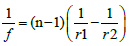 (2)
(2)
Where r1 and r2 are the radii of curvatures of the two surfaces of the lens and n is the refractive index of the material of the lens. If we consider biconvex lens and take r1=r=-r2, the Equation 2 gives focal length as
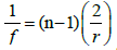 (3)
(3)
If the refractive index is intensity dependent as given in Equation 1, then the focal length will also be dependent on the intensity of the incident light. Thus, the intensity dependent focal length of the lens can be written as (using Equation 1 in 3)
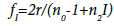 (4)
(4)
Now when the incident light intensity I=0, the focal length becomes
 (5)
(5)
Equations 4 and 5 show that fI < f0, so the direction of propagation will be changed (Figure 1). If light of intensity >I is incident, the focal length becomes smaller and this can be utilized for all optical switching. The change in focal length is given by
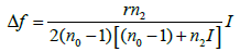 (6)
(6)
The angular deviations are calculated from the relation
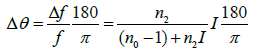 (7)
(7)
It is interesting to note that, the angular deviations are independent of the geometry of the lens but depend on the intensity of the incident light only.
Analysis of the Switching of NKL
To analyze the switching of the NKL designed in the section 2 above we consider radius of curvature r equal to 1m, and parameters of CS2 given in the Table 1, i.e. n0 = 1.63, n2 = 3.2 x 10⁻¹⁸ m2/W. With these parameters the focal length without light becomes f0 = 0.79 m. The variation of focal length with the intensity of light is shown in the Figure 2. From Figure 2, it is clear that the focal length changes from 0.79 m to 0.70 m for an incident light of intensity 2 x 10¹⁶ w/sqm, a change of 13% approximately.

Figure 2: Variation of focal length with intensity.
In the Figure 3, the change in focal length is plotted against intensity of the incident light. For small intensities, the variation is almost linear. This property signifies the fact that if intensity doubles the change in focal length also doubles and very suitable for switching the light signals in different paths. This is also confirmed by the angular deviation produced by the lens as shown in the Figure 4. So for lower intensities better performance can be achievable. The nonlinear lens compared to nonlinear slab [6] obtains a greater angular deviation 47 degrees. Therefore, a lens shows better performance compared slab.

Figure 3: Variation of change in focal length with intensity of light.

Figure 4: Variation of angular deviation with intensity of incident light.
From the above analysis, it is clear that considerable change in focal length and angular deviation is achieved with light intensity of the order of 1016 w/sqm.
Implementation of Different all Optical Logic Gates and Logic Processors
A single nonlinear Kerr Lens (NKL) designed above is used to implement different logic gates and processors in a single module. The module is shown in the Figure 5. Here A, B, and are three inputs, combined and made incident in the nonlinear lens, P. Depending on the number of inputs the optical signals are routed to different paths PO1, PO2 and PO3. When only a single optical signal is present the light is routed along PO1, when any two of the input signals A, B and C are present, the optical signal is routed along PO2, and when all three inputs are present simultaneously, the light is routed along PO3. These three different paths are further combined to generate six overall outputs to generate different logic gates and logic processors. In the Table 2, inputs and different output conditions are given. From the table it is clear that if we consider the input C as control, we can generate AND, NOR, NAND, X-OR and X-NOR gates with A and B as input and if we consider three input cases then 3-input AND, 3-input X-OR and 3-input majority function can be designed as explained below with reference to Figure 5.
| INPUTS | OUTPUTS | |||||||
|---|---|---|---|---|---|---|---|---|
| C | A | B | O1 | O2 | O3 | O1 +O2 | O1+O3 | O2 +O3 |
| 0 | 0 | 0 | 0 | 0 | 0 | 0 | 0 | 0 |
| 0 | 0 | 1 | 1 | 0 | 0 | 1 | 1 | 0 |
| 0 | 1 | 0 | 1 | 0 | 0 | 1 | 1 | 0 |
| 0 | 1 | 1 | 0 | 1 | 0 | 1 | 0 | 1 |
| 1 | 0 | 0 | 1 | 0 | 0 | 1 | 1 | 0 |
| 1 | 0 | 1 | 0 | 1 | 0 | 1 | 0 | 1 |
| 1 | 1 | 0 | 0 | 1 | 0 | 1 | 0 | 1 |
| 1 | 1 | 1 | 0 | 0 | 1 | 0 | 1 | 1 |
Table 2: Inputs and outputs conditions of the module of Figure 5.

Figure 5: Module for logic gates and processors using single NKL.
Two input AND gate
If we consider input C as control and set C=0, i.e. no light signal is present, the output O2 is the operation A AND B as clear from the Table 2. Let us explain the operation of the logic gate AND.
When C = 0, four different conditions are possible.
A=0, B=0. In this condition, no signal is present in any of the output and hence the output O2 is zero.
A=0, B=1. In this condition since only a single input is present, the light will travel along the path PO2 of Figure 5 making output O2 high, i.e. 1.
A=1, B=0. In this condition also only a single input is present. Hence the light will travel along the path PO2 of Figure 5 making output O2 high, i.e. 1 again.
A=1, B=1. Since both inputs are high, the light will travel along the path PO3, so there is no output in O2, giving low state.
So the module behaves like a two input AND gate. Again O2 + O3 is also gives A AND B operation.
Two input X-OR gate: When C=0, the output O1 is X-OR operation of A and B. In this situation four different input conditions are possible.
A =0, B=0, no signal is present in any of the output. So O1 is also zero (0).
A=0, B=1, signal is present in the output O1 as the light travels along the path PO1 giving high output.
A=1, B=0. In this condition also, the output is present at O1.
A=1, B=1, the light signal travels along the path PO2, giving no output at O1. So the output is zero again.
So when C=0, the output O1 generates X-OR operation of A and B. It is interesting to note that O1 + O3 is also generates X-OR operation of A and B.
Two input NOR gate: To get operation of a two input NOR gate, we have to make C = 1, i.e. high. In this situation, the output O1 gives the operation of NOR gate as clear from the Table 2. Let us consider the four different cases:
A=0, B=0. In this condition, only one input signal(C in this case) is high, so the light will follow the path PO1 giving a high (1) output.
A = 0, B=1, so that two inputs(taking C also) are high and the light signal follows the path PO2, so that output O1 is low i.e. zero(0).
A=1, B=0, so that again two inputs are high such that the light ray travels along PO2, so that output O1 is again low(0).
A=1, B=1, in this condition all the three inputs are high and the light travels along the path PO3 from the lens, NKL.
Two input X-OR gate: When C=1, the output O2 gives the operation of X-OR gate between A and B and is clear from the Table 2. This can be explained considering the following cases:
A =0, B=0, only one input signal is present, so output O2 is zero (0).
A=0, B=1, two input signals are present and hence the output O2 is high as the light travels along the path PO2.
A=1, B=0. In this condition also, the output is present at O2 due to two high inputs A and C.
A=1, B=1, the light signal travels along the path PO3, giving no output at O2. So the output is zero again.
It is interesting to note that we can generate X-OR gate for c=0 and C=1 from different outputs.
Two input AND gate: When C=1, the output O3 gives AND between A and B. In this condition four different cases occur. When:
A=0, B=0, only one input C is high sending light along PO1 so that no signal in the output O3. i.e. 0 output.
A=0, B=1.
A=1, B=0, in these conditions two inputs are high routing the light along PO2, and no output at O2.
A=1, B=1, in this condition all the three inputs A, B, and C are high and the light travels along PO3, so the output O3 is high.
This is nothing but the A and B operation when C=1. It is interesting to note that output O2 is AND gate output when C=0.
Two input NAND gate: In the condition C=1, the output combination O1 + O2 is nothing but X-NOR of A and B as clear from the Table 2. There are four different conditions:
A=0, B=0, so only one input signal C is high (1) and the light travels along the path PO1 making O1 + O2 high, i.e. 1.
A=0, B=1, so two inputs B and C are high sending light along the path PO2 making O1 + O2 high again.
A=1, B=0, so again two inputs A and C are high making O1 + O2 high as light from the lens travels along PO2.
A=1, B=1, so that all three inputs A, B and C are high routing the light along PO3. This makes O1 + O2 low as no light along PO1 and PO2.
Two input X-NOR gate: When C=1, the combination O1 +O3 generates A X-NOR B operation and can be explained in the following way.
A=0, B=0 , only one input C is high sending light along PO1 so that sending light signal to the output O3 and making O1 + O3 high.
A=0, B=1.
A=1, B=0, in these conditions two inputs are high routing the light along PO2, and no output at O1 and O3. So the output O1 + O3 is low (0).
A=1, B=1, in this condition all the three inputs A, B, and C are high and the light travels along PO3, so the output O1+ O3 is high.
This is nothing but the A X-NOR B operation when C=1.
Three input AND gate: From the table it is clear that if we consider the output O3, it will give AND operation of three inputs A, B and C. If any one of the three inputs A, B, and C is low, there will be now output in the path PO3, making output O3 low, i.e. zeros (0). The output O3 is high only when all the three inputs are high because in this condition only the light propagates along PO3 from the lens, NKL. This is nothing but the AND operation of A, B and C.
Three input X-OR gate: The output combination O1 +O3 gives three input X-OR operation of A, B and C. There are eight different cases.
A=0, B=0, C=0. Since all the inputs are low, no light in any of the output making O1 +O3 low.
A=0, B=0, C=1.
A=0, B=1, C=0.
A=1, B=0, C=0, in these three conditions only one input is high. So light will travel along PO1, making the output O1 +O3 high.
A=0, B=1, C=1.
A=1, B=0, C=1.
A=1, B=1, C=0, in these three conditions two inputs are high so light travels along PO2, so that O1 +O3 is low.
A=1, B=1, C=1, all the inputs are present and the light is routed along the path PO3, making output O1 +O3 high.
So it is found that the output O1 +O3 is high only when odd number of inputs are high which is the property of X-OR operation.
Three input majority gate
A majority gate gives output, the majority of the input condition. If majority of the input is 0, the output is zero and if majority of the input are high, i.e.1, the output is high. This is also called majority function or majority vote. The operation can be obtained by combination O2 + O3.
In the input conditions (i). A=0, B=0, C=0. (ii). A=0, B=0, C=1, (iii). A=0, B=1, C=0, (iv). A=1, B=0, C=0, the majority are 0 or low inputs. In these conditions no light travels along the path O2 or O3, making output O2 + O3 low, i.e. majority input.
For others conditions (v) A=0, B=1, C=1, (vi). A=1, B=0, C=1, (vii). A=1, B=1, C=0, (viii). A=1, B=1, C=1, majority of the input is high. For conditions (v) to (vii), the output O2 is high and for the condition (viii), the output O3 is high. So for all four conditions (v) to (viii) the combination O2 + O3 is high as majority of the inputs are high.
Half Adder
A half adder adds two single bits A and B and generates carry=A AND B and SUM=A X-OR B. As explained in section 4.1 and 4.2 of this communication when input C=0, the outputs O2 and O1 produces CARRY and SUM respectively. Similarly when C =1, the CARRY and SUM are generated from outputs O3 and O2 as shown in the block diagram of Figure 6. So in both the conditions of C=0, and C=1 we have half adder operation. So the module can simultaneously gives three input logic gates and half adder. In Figure 6, when C=0, O1 gives the SUM and O2 gives the CARRY. But when C=1, O2 gives the SUM and O3 gives the CARRY of the half adder. The operation of the half adder can be easily verified from the Table 2.

Figure 6: Half Adder.
Implementation of the full Adder
The CARRY of a Full Adder is nothing but the majority vote of two input bit A and B and the CARRY of the previous addition which is denoted by C in this case. The sum of a Full Adder is the X-OR operation of the two input bits A and B, and CARRY, C of the previous addition. In logical form
SUM = A X-OR B X-OR C and
CARRY = AB + AC + BC (Majority Function gate).
As explained in section 4.9, the output combination O1 +O3 gives three input X-OR operation of A, B and C and in section 4.10, it is explained that the three input majority function can be generated from the combination O2 + O3. Therefore, the full adder block can be drawn as Figure 7. The operation of the full adder is clear from the Table 2.

Figure 7: Full Adder
Conclusions and Discussions
The design and analysis of a nonlinear Kerr lens using Carbon di Sulfide (CS2) is explained. Nonlinear properties of few other important materials are also included. The variation of nonlinear focal length, change in focal length and angular deviation is plotted against intensity of incident light and better performance in comparison to slab type of nonlinear material in terms of deviation of light is obtained. The deviation produced by the lens is not dependent on the angle of incidence as in nonlinear prism. Further, we can engineer the lens by changing the radii of curvature of the refracting surfaces as well. The most interesting characteristics of the proposed module is that, it can generate all the logic gates, i.e. two input AND, X-OR, NAND, NOR, X-NOR, three input AND, X-OR and majority function and optical processors half Adder, Full Adder simultaneously. Another interesting fact about the module designed in this communication is that two input logic gates can be implemented in a controlled way, i.e. when C=0, one output gives a two input logic gate and for C=1, the same output gives another logic gate. This confirms reconfigurability of the logic gates also. For example, when C=0, O1 generates X-OR operation but when C=1, it generates NOR operation as clear from the sections 4.2 and 4.3. This is true for other outputs also. This property of the output O2 gives very interesting property to the Half Adder. By controlling the input C one can generate SUM and CARRY of the half Adder from a single output O2. This is possible because O2 gives X-OR operation (SUM) when C=0 and gives AND operation (CARRY) when C=1 respectively. The device presented in this communication can be used as a binary logic and arithmetic unit that can generate all functionalities simultaneously and can demand novelty in its own characteristics.
References
- Lovkesh, Marwaha A (2015) Implementation of optical logic gates at 160 Gbps using nonlinear effect of single SOA. Optics and Laser Technology 70: 212-218.
- Tang Y, Chen Y, Jiang H, Ji W, Wu Y, et al. (2013) Proposals for simultaneous all-optical AND, NOR, and XNOR using QPM cascading nonlinear effects in two PPLNs. Chin Opt Lett 11: 061901.
- Wang J, Yang JY, Huang H, Willner AE (2013) Three input optical addition and subtraction of quaternary base numbers. Opt Express 21: 488-499.
- Mukherjee K (2013) Method of implementation of all optical tri-state logic in frequency encoded format using non-linear material. Optik 124: 2807-2810.
- Mukherjee K, Ghosh P, Kumbhakar D, Meikap AK (2010) A method of optical implementation of frequency encoded all optical logic gates based on multiphoton processes in nonlinear material. Opt Quant Electron 42: 121-128.
- Sarkar T, Chattopadhyay T (2012) Kerr nonlinear prism as all- optical switch. Proceeding of MDCCT 193-195.
- Zhang J, Xu H (2009) Optical computation based on nonlinear total reflectional optical switch at the interface. Pramana 72: 547-554.
- Mukherjee K (2011) A method of implementation of frequency encoded all optical logic gates based on non-linear total reflectional switch at the interface. Optik-International Journal for Light and Electron Optics 122: 1284-1288.
- Mukherjee K (2011) On the method of implementation of frequency encoded all optical reconfigurable logic gates based on total reflectional swith at the interface. Optics and Photonics Letters 4: 25-34.
- Cowdgury KR, Mukhopadhyay S (2008) An all optical scheme of signed digit binary addition based on optical nonlinear material. Optoelectron Lett 4: 0447-0451.
- Bhattacharya LS, Patra SN, Mukhopadhyay S (2015) An all optical prototype neuron based on optical Kerr material. Optik 126: 13-18.