Research Article, J Electr Eng Electron Technol Vol: 6 Issue: 2
Digitally-Controlled Frequency Generation Using Variable-Length Ring Oscillators
Linda Gong* and Gary H Bernstein
Department of Electrical Engineering, University of Notre Dame, Notre Dame, IN 46556 USA
*Corresponding Author : Linda Gong
Department of Electrical Engineering, University of Notre Dame, Notre Dame, IN 46556 USA
Tel: 574-631-6269
E-mail: lgong@nd.edu
Received: April 24, 2017 Accepted: June 12, 2017 Published: June 18, 2017
Citation: Gong L, Gary H Bernstein (2017) Digitally-Controlled Frequency Generation Using Variable-Length Ring Oscillators. J Electr Eng Electron Technol 6:2. doi: 10.4172/2325-9833.1000144
Abstract
A simple variable-length ring oscillator (VLRO) in which a selectable number of inverters is shunted using bypass transistors is introduced. A range of frequencies can be selected by activating or deactivating the bypass circuitry. LTspice simulations demonstrating the performance are presented. BSIM4 transistor models using 50nm gate lengths are used in the design of the inverters and bypass transistors. The fundamental frequency generated by each VLRO is determined via Fourier transforms of the output square wave. The data show that the VLRO can effectively generate a wide range of frequencies in a large number of steps based on the selection of bypass transistors that are activated. The prototypical circuit presented here uses 45 CMOS inverters to generate a range of frequencies between about 0.56 GHz and 1.4 GHz. Four different VLROs that demonstrate the ability to synthesize frequencies based on external inputs are presented. Based on the chosen VLRO design, anywhere from 6 to 16 unique frequencies can be selected over the frequency range.
Keywords: Ring oscillators; Clock frequency synthesis; DDFS; CMOS design;Wireless communication; Digital logic
Introduction
With the growth of mobile technology, there is a strong effort to find digital replacements for formerly analog circuits. Modern wireless communications, data processing systems, and mobile phones require frequency synthesizers that can be easily integrated with CMOS designs [1-18]. Radio frequency (RF) generators are traditionally analog, but there is a push to develop digital alternatives [19]. In addition, reduced supply voltages and a move to CMOS integration has created difficulties for traditional analog RF designs such as charge pumps [20-22].
Previous work on frequency generators falls into three categories [3,19] viz., phase-locked loops (PLL) [8,10,15,23], fractional frequency synthesizers (FFS), and direct digital frequency synthesizers (DDFS) [12,13,24]. Frequency generators involving the use of PLL have been created using inductors, capacitors, and resistors [7,16,25]. Other PLL use a large number of transistors to implement accumulators [15], loop filters [15,23,26], and multiplexers [26]. DDFS are more space- and cost-efficient than their RF predecessors [2,5,6,11,16,25]. In addition, DDFS systems have less noise than PLLs [11]. Other DDFS designs incorporate the use of a large number of transistors for accumulators [3,11,27], multiplexers [1,3,5,11] registers [3,11,27], and other CMOS logic gates [1,2,3,5,11,14,27].
Ring oscillators (RO) are often used as building blocks in DDFS circuits because they are compact and easily integrated with CMOS technology [4,6,28]. There has been a significant amount of research done on ring oscillators, as they are useful for the evaluation of new devices, in high-clock-frequency microprocessors, and for clockfrequency synthesis [23,29]. In this paper we present a novel DDFS in the form of a variable-length ring oscillator (VLRO) as a candidate for dynamic frequency scaling (DFS). VLRO is a class of ROs in which the frequency is adjusted by changing the number of active inverters [1,4,5]. Our novel VLRO is simple, compact, and has the ability to generate a wide range of frequencies using CMOS devices without the use of passive components, multiplexers, or other complex digital logic circuits. Instead, we create a VLRO by adding bypass transistors to a simple RO that selectively excise the participation of some number of inverters, effectively changing the VLRO length and, therefore, its oscillation frequency.
We present simulations that demonstrate the operation of a prototypical VLRO including its range of frequency selectivity and available number of discrete frequencies based on the number of active RO stages (inverters). We refer to an RO with no bypass circuitry as an “intrinsic” RO. The length of the VLRO, in total number of inverters, is its “base” length, NB, and the number of functioning inverters, with some bypassed, is its “active length,” NA.
We describe here a prototypical VLRO of NB=45 using 50-nm gate lengths that oscillates with a range of frequencies from about 0.56 GHz to 1.4 GHz, or a frequency ratio of 2.5, in 16 steps. A previously reported design [2] can provide a slightly larger frequency range (0.30 – 1.4 GHz), but does so at the cost of significantly morecomplex circuitry. That design, which uses pass-gates as variable resistances for added delays, has a larger frequency ratio of 4.667, but only allows for selection between 11 frequency steps. In addition, the waveforms produced by the design are inherently trapezoidal due to the increased rise time added by the resistance, and must be converted back to a square wave to be useful. Another DDFS design [5] also has a large frequency ratio of 13, but the frequencies generated are between 0.001 and 0.013 GHz, which is significantly lower than the frequencies generated by our design, and also uses considerably more-complex circuitry. The RO design of [1] is similar to ours in frequency range and ratio, but allows only for switching between three frequencies, and also is more complex. The ROs of [14] are closer in simplicity to our design, but have smaller frequency ranges and frequency ratios of only 1.3. In addition, those RO designs provide only 7 frequency steps, which is significantly fewer than the 16 steps demonstrated by our prototypical design, which in fact could be much larger. The design of [2] incorporates transmission gates to adjust the speed of the ring oscillator. However, the transmission gates were used as tunable resistors, which introduced an analog component into the circuit. The usage of bypass transistors avoids this analog tuning, and allows for the frequencies to remain digitally controlled. In this paper, we present a VLRO DDFS that has the ability to synthesize relatively high frequencies over a wide range without compromising the number of selection steps or circuit simplicity.
VLRO Circuit Description
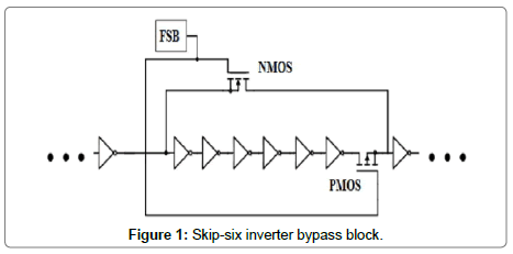
Our DFS scheme is based on circuitry that enables the bypassing of a preselected number of inverters in an RO in order to synthesize a wide range of frequencies in a large number of steps. The bypass circuitry comprises only two transistors that include one NMOS transistor in parallel, and one PMOS transistor in series, with the selected inverters to be omitted from the overall base RO length. Figure 1 shows a segment of a VLRO in which a frequency-select bit (FSB) selectively includes or omits an even number of inverters (by way of example six inverters is shown) from the total VLRO length, for a change in total period of the VLRO equal to approximately that of six inverter delays.
When the control bit is low, the NMOS transistor is off and the PMOS transistor is on. This action selectively routes the signal path through the block of inverters and the PMOS transistor, retaining the delay of the block of inverters in the total VLRO period. When the control bit is high, the activity of the bypass transistors is reversed, and the signal flows around the block of inverters, thus decreasing the total VLRO period. The FSB shown is one of many that can be used to address multiple bypass blocks, and would be the output of a separate frequency-select circuit that is not discussed in this paper.
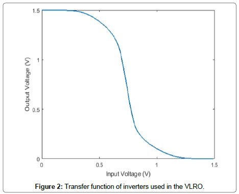
We use LTspice [30] for simulations, and start with, by way of example, a standard RO of base length NB=45 inverter stages in order to demonstrate a moderately sized circuit given the limitations of simulation times. Larger circuits having many more stages are feasible in practice, but a VLRO of 45 inverters was chosen for practical simulation purposes. We chose the BSIM4 transistor model [31] at 1.5 V for NMOS and PMOS transistors having 50-nm gate length and 0.5 μm and 1.0 μm widths for the NMOS and PMOS, respectively. Bypass transistors were sized to match the widths and lengths of the PMOS/NMOS transistors that comprise the inverters. The frequency generated by the VLRO's was measured for bypass transistors having different widths. Matching transistor sizes allowed for the generation of higher frequencies. The simulated voltage transfer function (VTC) for the inverter is shown in Figure 2.
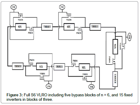
We define m to be the number of bypass blocks in a VLRO and n to be the number of inverters bypassed in each block. Figure 3 shows a full VLRO with m=5 bypass blocks, each one bypassing n=6 inverters, which we also refer to as “skip 6” or “S6”, for a total number of active inverters, NA, ranging from the circuit having NB=45 inverters to NA=NB – m*n=15 in 5 steps of n=6. This VLRO, therefore, has an associated six different oscillation frequencies, including the base frequency; the possible values of NA for this example are 45, 39, 33, 27, 21 and 15. The fifteen inverters without bypass circuitry, called “fixed inverters,” are distributed as five blocks of three placed between the five bypass blocks. To first order, the placement of the fixed inverters does not affect the overall performance, but in an actual circuit may have a small effect, which is not investigated in this paper. Also, the FSBs are represented as power supplies with values of 0 V or 1.5 V. It is assumed that appropriate logic can be added that will select various combinations of n-length bypass blocks for frequency selection.
Simulations were performed on the circuit of Figure 3 as well as variations for n=6, 4 and 2, called S6 (skip 6), S4, and S2, with fixed inverters interspersed approximately equally amongst the bypass blocks. For each simulation, some number of bypass blocks were selectively excised or included, ranging from 0 to 5 for S6, from 0 to 7 for S4, and 0 to 15 for S2.
An important variation comprises four different n lengths within one VLRO. In this “variable-skip” VLRO, VS-VLRO, there are four bypass blocks, each of which skips a different number of n inverters (S2, S4, S8 and S16) that can be combined to allow any even number between 0 and 30. This VS-VLRO structure allows for the selection of a larger number of frequencies, the same as that of the S2 ring oscillator, but requires fewer FSBs and associated circuitry. Unlike the S2 VLRO, which has 15 bypass blocks, the prototype VS-VLRO has only four bypass blocks, yet achieves the same number, viz., 16, of different frequencies. Compared with fixed skip lengths, the VSVLRO, therefore, offers the benefit of the same frequency range for a given NB, but uses fewer bypass blocks and associated number of FSBs while achieving a larger number of discrete frequencies.
Simulation Results
LTspice was chosen to design and simulate our circuit behavior for its wide selection of predefined components. The BSIM4 transistor model is used in the design of all of our VLROs. Building real circuits is beyond the scope of this work, which is intended only to demonstrate the basic operation and utility of the VLRO and VSVLRO architectures.
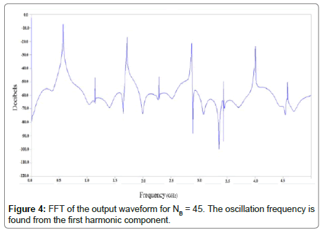
To analyze the VLRO design, the program’s display and fast Fourier transform (FFT) functions were used to determine the frequency output of each circuit. The output node remains the same for all simulation runs, and is located after the first block of bypassed inverters. The oscillation frequency was taken as the fundamental frequency of the FFT, which was more precisely identified compared with using the waveform in the time domain. Figure 4 shows the lowest few harmonics of the FFT from which the frequency was determined for NB=45.
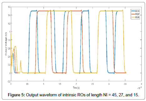
First, the frequencies of intrinsic (i.e., having no bypass blocks) ring oscillators were measured to demonstrate the behavior without the addition of any bypass circuitry. Six intrinsic ROs were simulated with NI=45, 39, 33, 27, 21, and 15. Due to the absence of bypass transistors, and their associated resistances, in these intrinsic ring oscillators, the frequency for each intrinsic RO is higher than that of its VLRO counterpart. Figure 5 shows the output waveform of intrinsic ROs of lengths 45, 27, and 15. The figure shows the decreasing period of the waveform as the number of inverters decreases.
By turning on/off various bypass transistors using the FSBs, various VLRO lengths NA were selected, and simulations were performed for each length. The VLRO was adjusted between 45 and 15 inverters, at different intervals depending on the total number of inverters being skipped in each design. For the S6 VLRO, frequencies were determined at active lengths of 45, 39, 33, 27, 21 and 15 inverter stages. S4 and S2 lengths were simulated every 4 and 2 inverters, respectively.
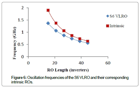
The data shown in Fig. 6 demonstrate that the frequency and time delay of the VLRO can be adjusted significantly based on the addition or removal of bypass blocks. However, due to the added channel resistance of the bypass transistors, and the associated additional RC delay, the frequencies generated by the VLRO are lower than those of the intrinsic ROs for each corresponding length. Figure 6 illustrates the difference in frequencies generated between the S6 VLRO and its corresponding intrinsic RO.
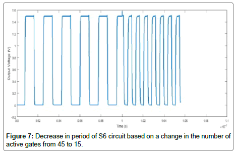
Figure 7 shows an output waveform of an S6 circuit that switches to a higher frequency based on a change in active stages from 45 to 15. At 100 nanoseconds, the FSBs are changed from low to high, causing five inverter blocks that are six inverters long to be bypassed, and the period of the waveform decreases from 1.8 ns to 0.73 ns (0.56 GHz to 1.46 GHz, respectively).
The S6 VLRO experiences a linear change in period as a function of the number of active stages. The constant offset between periods of the intrinsic ROs and VLROs is due to the fact that the bypass transistors contribute a constant delay to each stage regardless of whether that stage is on or off. One of the bypass transistors, either NMOS or PMOS, will always be on and contribute a resistance to the signal path, decreasing the overall switching speed. Each transistor adds resistance to the signal path, which increases the delay, τ , by an amount τ=RC, where R is the channel resistance of the bypass transistor and C is the capacitance looking into the input gates of an inverter stage.
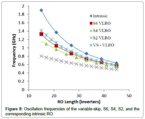
To further demonstrate the impact of the bypass blocks, S4 and S2 VLROs were created that bypass four and two inverters, respectively. This allows the NB=45 VLRO to generate a larger number of discrete frequencies at the cost of a larger number of FSBs and greater additional delay, as compared with the S6 VLRO. Figure 8 compares the output frequencies for the intrinsic, S2, S4, S6 and VS-VLRO designs. The data show that by reducing the number of inverters in each bypass block while increasing the number of FSBs, a larger number of discrete frequencies can be generated from the VLRO. More bypass transistors are needed to accommodate the additional bypass blocks, which increases the RC delay and results in a decrease in the overall speed of the VLRO. The S2 VLRO has the highest delay, and therefore runs slower than the S4 and S6 VLROs. The different VLROs have possible applications that may depend on the users’ specifications and needs; for example, the S2 VLRO might be used in designs that require a greater number of frequencies at lower speeds, while the S4 and S6 VLROs might be useful in applications that require higher clock frequencies, but not necessarily the same amount of flexibility in frequency selection.
The VS-VLRO has bypass blocks of four different values of n (inverters in a block), and allows for the same number of frequency selections as the S2, but with fewer FSBs and without as much additional time delay. This results in a VLRO with the frequency selection flexibility of the S2 and speeds greater than that of the S6 VLRO. Since the VS-VLRO has only four bypass blocks, there are fewer bypass transistors in the circuit, and thus, less additional delay. The frequency outputs for all possible values of NA for the VS-VLRO are compared with the intrinsic, S6, S4, and S2 frequencies in Figure 8.
Summary and Conclusions
In this paper, we demonstrate a novel variable-length ring oscillator topology for generating a range of oscillation frequencies with high selectability. In our prototype circuits, we use bypass transistors in combination with inverter blocks to synthesize frequencies between about 0.56 GHz and 1.4 GHz. Our variableskip topology offers additional flexibility and extended selectivity of available frequencies. Our results demonstrate that the design can successfully switch between frequencies based on changes to control bits. The results were obtained using LTspice’s circuit simulation toolbox, using the BSIM4 transistor model. The proposed VLROs can be used for highly-selectable, easily-integrated, and size-efficient clock frequency generation.
Physical-circuit results will differ based on the chosen transistor technology and physical layout of the VLRO. The addition of models for on-chip interconnects would likely result in different performance of the overall circuit operation. We would anticipate faster operation for shorter gate lengths, but some additional delays due to the inclusion of interconnect resistance and capacitance. We used an intrinsic RO length of 45 inverters for simulations due to practical limitations of required simulation times. A larger number of inverters and bypass blocks will yield a wider range of output frequencies. Conversely, the number of inverters and bypass blocks can be decreased to generate a smaller range of output frequencies at higher speeds. Higher VLRO speeds may also be achieved via the implementation of smaller and faster NMOS/PMOS transistors compared with those used in our simulations. Although the actual range of frequencies will depend on the particular technology chosen for implementation, we expect that the relationships between the oscillation frequencies will be consistent with the results presented here.
Acknowledgements
The authors would like to thank Dr. J. Chisum and Dr. A. Kriman for helpful discussions.
References
- Bui HT (2008) Design of an All-Digital Variable Length Ring Oscillator (VLRO) for Clock Synthesis. IEEE International Symposium on Circuits and Systems, Seattle, WA, USA.
- Nguyen MH, Pham CK (2010) A Wide Frequency Range and Adjustable Duty Cycle CMOS Ring Voltage Controlled Oscillator. International Conference on Communications and Electronics, Cape Town, South Africa.
- Mair H, Xiu L (2000) An Architecture of High-performance Frequency and Phase Synthesis. IEEE J Solid-State Circuits 35: 835-846.
- Mandal MK, Sarkar BC (2010) Ring Oscillators: Characteristics and Applications. Indian Journal of Pure & Applied Physics 48: 136-145.
- Mandal MK, Mondal H (2013) Design of Variable Length Ring Oscillator for Clock Synthesis. Third International Conference on Computational Intelligence and Information Technology, Mumbai, India.
- Parvisi M, Khodabakhsh A, Nabavi A (2008) Low-power High-tuning Range CMOS Ring Oscillator VCOs. IEEE International Conference on Semiconductor Electronics, Johor Bahru, Malaysia.
- Anand SB, Razavi B (2001) A CMOS Clock Recovery Circuit for 2.5-Gb/s NRZ Data. IEEE Journal of Solid-State Circuits, 36: 432-439.
- Chung C, Lee C (2003) An All-digital Phase-locked Loop for High-speed Clock Generation. IEEE Journal of Solid-State Circuits 38: 347-351.
- De Caro D, Strollo AGM (2005) High-performance Direct Digital Frequency Synthesizers in 0.25 /spl Mu/m CMOS Using Dual-slope Approximation. IEEE Journal of Solid-State Circuits 40: 2220-2227.
- Hsieh GC, Hung JC (1996) Phase-locked Loop Techniques- A Survey. IEEE Transactions on Industrial Electronics 43: 609-915.
- Ibrahim SH, Ali SH, Islam S (2014) Hardware Implementation of 32-Bit High-Speed Direct Digital Frequency Synthesizer. The Scientific World Journal 2014: 1-9.
- Wu J, Chen J, Wu D, Zhou L, Jiang F (2013) A 4 GHz 32 Bit Direct Digital Frequency Synthesizer Based on a Novel Architecture. Journal of Semiconductors 34: 2- 6.
- Nosaka H, Yamaguchi Y, Yamagishi A, Fukuyama H, Muraguchi M (2001) A Low-power Direct Digital Synthesizer Using a Self-adjusting Phase-interpolation Technique. IEEE Journal of Solid-State Circuits 36: 1281-1285.
- Kumar M (2013) A Low Power Voltage Controlled Oscillator Design. ISRN Electronics 2013: 1-6.
- Staszewski RB, Balsara PT (2005) Phase-domain All-digital Phase-locked Loop. IEEE Transactions on Circuits and Systems II: Express Briefs 52: 159-163.
- Bashir I, Staszewski RB, Balsara PT (2016) A Digitally Controlled Injection-Locked Oscillator with Fine Frequency Resolution. IEEE Journal of Solid-State Circuits 51: 1347-1360.
- Staszewski RB, Wallberg JL, Rezeq S, Hung C, Eliezer OE (2005) All-Digital PLL and Transmitter for Mobile Phones. IEEE Journal of Solid-State Circuits 40: 2469-2482.
- Guo Z, Tang X, Xiao S (2010) An 8~20 GHz Wideband Frequency Synthesizer. 2010 International Symposium on Intelligent Signal Processing and Communication Systems, Chengdu, China.
- Noel DP, Kwasniewski TA (1994) Frequency Synthesis: A Comparison of Techniques. Electrical and Computer Engineering CCECE-94, Halifax, United Kingdom.
- Sotiriadis PP, Miliou N (2014) Single-Bit Digital Frequency Synthesis via Dithered Nyquist-Rate Sinewave Quantization. IEEE Transactions on Circuits and Systems I: Regular Papers 61: 61-73.
- Staszewski RB (2010) State-of-the-art and Future Directions of High-performance All-digital Frequency Synthesis in Nanometer CMOS. IEEE International Symposium on Circuits and Systems, Paris, France.
- Staszewski RB, Hung C, Leipold D, Balsara PT (2003) A First Multigigahertz Digitally Controlled Oscillator for Wireless Applications. IEEE Transactions on Microwave Theory and Technique 51: 2154-2164.
- Young IA, Greason JK, Wong KL (1992) A PLL Clock Generator with 5 to 110 MHz of Lock Range for Microprocessors. IEEE Journal of Solid-State Circuits 27: 1599-607.
- Xiu L (2008) The Concept of Time-average-frequency and Mathematical Analysis of Flying-adder Frequency Synthesis Architecture. IEEE Circuits and Systems Magazine 8: 27-251.
- Sun L, Kwasniewski TA (2001) A 1.25-GHz 0.35-μm Monolithic CMOS PLL Based on a Multiphase Ring Oscillator. IEEE J Solid-State Circuits 36: 910-916.
- Kim JH, Kwak YH, Kim M, Kim S-W, and Kim C (2006) A 120-MHz–1.8-GHz CMOS DLL-Based Clock Generator for Dynamic Frequency Scaling. IEEE J Solid-State Circuits 41: 2077-2082.
- Geng X, Dai FF, Irwin JD, Jaeger RC (2010) An 11-Bit 8.6 GHz Direct Digital Synthesizer MMIC With 10-Bit Segmented Sine-Weighted DAC. IEEE Journal of Solid-State Circuits 45: 300-313.
- Jovanovic G, Stojcev M, Stamenkovic Z (2010) A CMOS Voltage Controlled Ring Oscillator with Improved Frequency Stability. Scientific Publications of the State University of Novi Paza 2: 1-9.
- Sasaki N (1980) Higher Harmonic Generation in CMOS/SOS Ring Oscillators. IEEE Transactions on Electron Devices 29: 280-83.
- http://www.linear.com/designtools/software/
- http://www-device.eecs.berkeley.edu/bsim/?page=BSIM4
 Spanish
  Chinese
  Russian
  German
  French
  Japanese
  Portuguese
  Hindi
Hindi 