Spanish
  Chinese
  Russian
  German
  French
  Japanese
  Portuguese
  Hindi
Hindi Research Article, J Electr Eng Electron Technol Vol: 8 Issue: 1
Relationship between Jitter Variance, Lock Time and Phase Noise of A Second-Order PLL
Mazumdar D1*, Kadambi G2 and Vershinin Y1
1Coventry University, Scarborough, Ontario, Canada
2M. S. Ramaiah University of Applied Sciences, Bengaluru, India
*Corresponding Author : Mazumdar D
Coventry University, Scarborough, Ontario,Canada
E-mail: ionchannelequation@gmx.com
Tel: +(001) 437 345 0602
Received: November 23, 2018 Accepted: January 24, 2019 Published: January 31, 2019
Citation: Mazumdar D, Kadambi G, Vershinin Y (2019) Relationship between Jitter Variance, Lock Time and Phase Noise of a Second-Order PLL. J Electr Eng Electron Technol 8:1. doi: 10.4172/2325-9833.1000172
Abstract
This paper covers analytical relationships between phase noise, lock time and jitter variance. An expression is derived for Lock time in terms phase margin. Analytical expressions have been derived in this paper for the variation of Lock time with respect to Phase Margin and lock time with respect to its damping coefficient. Analytical expressions are derived for the jitter variance with respect to the phase margin of a second-order PLL. Analytical expressions are also derived for the derivative of jitter variance of a second-order PLL with respect to its phase margin. The jitter variance is plotted separately for time varying part of the jitter variance and time invariant part pf the jitter variance.
Keywords: Phase locked loop; Phase margin; Phase noisel Lock time; Jitter variance; Damping coefficient; VCO sensitivity
Introduction
Second-order PLLs comprise of four blocks. The first block is the Voltage-Controlled Oscillator (VCO) – an oscillator whose output frequency is a function of a control voltage applied at its input. Linear VCO models are used. The second block is a frequency divider block which is used to divide the VCO output frequency by a fixed quantity. Divider input is the VCO frequency of the PLL and divider output is the comparison frequency of the PLL. The third block is the Phase- Frequency Detector (PFD) which compares the phase shift between a reference frequency waveform (primary input) and the output of the divider. The time varying output of the PFD is filtered before the said output is applied to the VCO input. The fourth block of a secondorder PLL is a RC filtering block to filter the PFD output (Figure 1).

Figure 1: A DDS+DAC feeding a second-order PLL.
VCO sensitivity (Kv) is the ratio of output frequency of a VCO divided by the control voltage (input) measured in Hz/volt. PFD sensitivity (KÕ) -Measure of PFD output (usually control voltage) vs. phase difference at PFD input.
Divide ratio is the ratio of PLL output frequency (f2) divided by PLL comparison frequency (f1). It is an integer for integer divider PLLs and a fraction for fractional divider PLLs.
N = f2 / f1(1)
N is termed as the divide ratio of a PLL. f2 and f1 are the output and input frequency respectively.
Phase Margin (PM) is the excess phase shift in a PLL when the gain is unity. It’s a measure of relative stability of the PLL.
Damping Coefficient (DC,ζ ) is a PLL parameter that controls the nature of the oscillatory response of a PLL. Lower the DC the more oscillatory the response of the PLL to a step input. Underdamped PLLs have (DC <1), overdamped PLLs have (DC>1).
The natural frequency ( ωn ) for a second-order PLL is defined as a function of VCO sensitivity, PFD sensitivity, divide ratio and loop filter time constant.
Phase noise – The voltage of an oscillator in the presence of both random variations in amplitude and phase can be represented as:
V (t) = ( A+ v(t))cos (2π ft +Õ (t)) (2)
In Equation (2), A is the amplitude of the original frequency source. In turn,v(t) are the random fluctuations of amplitude, fois the center frequency of the frequency source, and φ (t) is the instantaneous value of random phase perturbation of the frequency source which gives rise to Phase noise.
Energy due to the phase perturbation term can be written as a square of the magnitude of Fourier Transform of the auto-correlation function of the phase variation.
S( f ) = | F ( φ ( t))|2 (3)
In Equation (3) F is the Fourier Transform operator. φ (t) is a random variable representing phase noise in time domain. Sφ ( f ) is Power Spectral Density (PSD) of jitter.
Absolute jitter is the difference between successive zero crossing times of a waveform after Lee [1].

In Equation (4), tn is the time of zero crossing at the end of nth cycle, nT is the cycle number (n) times nominal period (T), and j a, n is the absolute jitter in the nth cycle.
If the nominal period and zero crossing points for a time domain waveform are known, the period jitter can be defined as (Lee [1]),

In Equation (5), T is the nominal period of a waveform, tn is the zero crossing at nth cycle end, and t n+1 is the zero crossing in (n+1)th cycle. Sequence jn is the Period jitter of nth cycle.
Jitter variance is the time averaged variance of jitter the square of the amplitude of jitter-assumed to be a zero-mean process.
The transfer function which is the output to input ratio of the PLL in the ‘s’ domain of the second-order PLL with a first-order loop filter is written as:
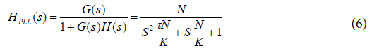
In Equation (6), G (S) is the Transfer function of the forward path of a PLL. In turn, HPLL (s) is the Transfer function of the PLL, H (S) is the Transfer function of the feedback path of a PLL, Kv is the VCO sensitivity (Hz/Volt), Kφ is the PFD Sensitivity, and K= KV KÕ is the product of VCO sensitivity and PFD Sensitivity. τ = RC is the time Constant of Loop filter and N is the feedback divide ratio
Converting Equation (6) to a generic transfer function one obtains the transfer function of a second order Type I PLL in terms of its them ωn and ζ as,
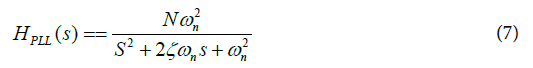
In Equations (6 and 7), the denominator polynomial is of the second order, which describes the PLL as a generic second order system. DC and natural frequency are defined for generic second order systems [2]. Some necessary terms that must be defined in this paper.
Noise Transfer Function (NTF) is the transfer function from a noise source to the primary output of a PLL [3].
Amornthrippart et al. [4] has discussed computation of phase noise in PLLs using phase noise sources and noise transfer function.
Daniels [3] has derived a piece wise linear model of a second order PLL. Daniels defines a new type of stability criterion for second order PLLs based on conservation of charge. Daniels [5] further extends his second order PLL work to third-order and fourth-order PLLs. However, the relationship between Phase noise and the referred performance metrics of PLL has not been explored in [5].
Drucker [6] has derived expressions for the noise transfer functions (NTF) of 4 different phase noise sources of arbitrary order PLL. Drucker [6] has discussed models of multiple noise sources without providing a closed form expression to compute the composite PSD (Phase Noise) at the output of PLL. Drucker [6] and He [7] did not relate the influence of performance metrics of DACPLL such as PM, settling time and damping coefficient on the phase noise of DAC-PLL.
Savic [8] considers the variation of PM with bandwidth of loop filter in a 3rd order PLL.
He [7] has provided an analysis of PM of second, third and fourth order PLL and the variance of lock time with PM.
Razavi [9] has described PLL transfer functions and provided insights into general phase noise analysis.
Golestan et al. [10] present higher order PLL design for power system applications. A systematic method for the design of higher order PLLs is described. It does not discuss theoretical issues with the roots of a third order or fourth order PLL.
Golestan et. al. [10] discusses three phase Frequency Locked Loops [FLLs] for power systems and provides models and stability analysis of three-phase second order FLLs. If power systems are imbalanced the instantaneous frequencies of each phase can be slightly different. A second order FLL tracks both frequency and its derivative in a imbalanced 3 phase system.
Herzel and Piz [11] have derived the NTFs for a fractional N PLL with the sigma-delta modulator in the feedback path. PLL model of Drucker [6] is easy to use to compute phase noise. Herzel [12] places the divider noise source is placed before the frequency divider, in this paper the noise source is placed after the frequency divider.
Herzel and Piz [11] have defined a system level simulation model for a 3rd order PLL using the phase noise of VCO as an Ornstein- Uhlenbeck type of process.
Hangmann [13] describes a third order event driven model for a digital PLL. His model describes very fast event driven behavioral model for higher order PLLs with comparable accuracy to a SPICE simulation.
Hangmann et al. [14] describe a difference equation approach for the analysis of a charge pump PLL which is target to for non-linear phase comparators. The authors claim their model is valid over a wider range of phase errors as compared to a linear model.
Gardner [15] derived two different stability criteria one for second order and another for third order PLLs. Which are called Gardner’s K.
Van Paemel [16] proposed a behavioral model for the design and analysis of charge pump PLLs. The Charge Pump-Phase Frequency Detector (CP-PFD) is a three-state device(UP state, DOWN state and a “NULL” state) that undergoes state transitions when the output state of the CP-PFD changes. If CP-PFD is in one of these states, then within that state the PLL can be described by linear state equations. Van Paemel [16] lists two state variables first being the pulse width of the phase detector and the second being the capacitor voltage of loop filter. These two state variables are used to compute the next pulse width of phase.
Carlosena [17] proposes a low-pass filter in a PLL termed as a Przedpelski Filter. He proposes an additional frequency feedback loop for accelerated locking.
Hedayat [18] extended Van Paemel’s [16] method to allow a variable time step enabling greater accuracy. Hedayat’s model requires six internal states but limited to fourth order PLLs.
Wang [19] has provided a method to suppress spurs in Fractional N PLLs using re-quantization methods.
Abramowitz [20] has provided the application of Lyapunov’s stability to third order PLLs. His model assumes a forward path with a non-linear sinusoidal phase detector.
Monteiro [21] has written about PLL stability and considered criteria for Hopf bifurcations in a 3rd order PLL.
Abdelfattah [22] performs an analytical and comparative study on the design of the loop filter in (PLLs). His method allows the design and component selection for various loop filters.
De Almeida et al. [23] proposes a new find of phase detector which replaces a multiplicative phase detector with a more generalized phase detector utilizing the q-product which demonstrates improved linearity and PLL pull-in. Kim et al. [24] describe and 1.35 GHz alldigital phase-locked loop (ADPLL) with an adaptively controlled loop filter. Adaptive Loop Gain Controller (ALGC) effectively reduces the nonlinear characteristics of the bang-bang phase-frequency detector (BBPFD).
Weigand et al. [25] has created a new technique for simulating a PLL with nonideal charge pumps featuring dead zones, current source mismatches, charge pump leakage, and nonlinear VCO transfer functions.
In a second-order system such as the PLL of the DAC-PLL, the PM is the value of the phase shift for which the amplitude gain is 0 dB or unity gain. In a PLL, PM of a second order system can be controlled by controlling the DC [26]. The DC determines how fast a second-order PLL can settle down after a unit step function is applied at the input of the PLL. Underdamped systems with DC<1 have faster rise times for step input, are oscillatory and exhibit lower PM. Overdamped systems with DC>1 are non-oscillatory with higher PM compared to underdamped systems.
The expression relating these parameters PM and DC of a secondorder PLL is given by Dorf [26].
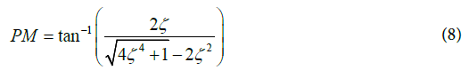
Equation (8) is an expression for the PM of a second-order PLL. The natural frequency of a second-order PLL is expressed in terms of KV Kφ, and time constant (τ ) ,
In Equation (10) the DC of the PLL is written as
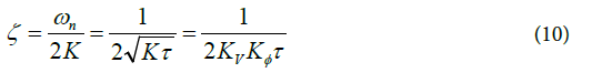
This paper seeks to answer whether there an analytical relationship between the Lock time of a second order PLL and its PM. The second question is there an analytical relationship between the derivative of the Lock time of a second order PLL and its PM. The third question is that what is the relationship between the jitter variance of a second order PLL and its PM. The fourth question is that what is the relationship of the variation of jitter variance with respect to the PM of a second order PLL. Now we extend the relationship between DC and PM.
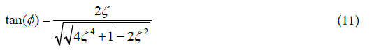
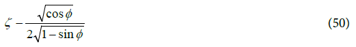
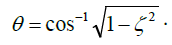
In Equation (11) φ is the PM of a second-order PLL and ζ is its DC. Inverting and squaring both sides of Equation (11) a new expression for the DC in terms of PM is obtained as
Lock Time and Phase Margin
Lock time of any PLL is defined as the time required in achieving an output frequency which is within a small but specified range of a desired output frequency when a frequency step of bounded size is applied to the PLL. A small lock time is necessary for communication systems such as UMTS (with switching time < 200usec. Lock time is inversely proportional to the PLL loop Band-Width (BW).
A closed-form expression relating lock time and DC of a secondorder Type II PLLs has been derived. Locking is achieved in a PLL when the output frequency of PLL approaches a specified frequency after the application of a frequency step to the PLL. An absolute frequency difference between the frequency of output of PLL and the target frequency, must be specified to define Lock Time.
The frequency step applied to the PLL must be within the lock range of the PLL which is defined as the maximum frequency range within which the PLL can track its input frequency. Lock time has been defined by Banerjee [2] as:
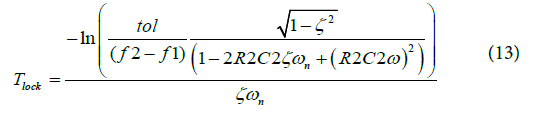
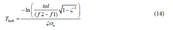
In Equation (13), T look is lock time of a second-order type I PLL. Tlock is the time required for PLL to reach an output value which differs from the final target frequency by a specified deviation (specified by tol). The frequency step applied to the PLL is (f2-f1) (Hz). T2=R2C2 is the time constant of the PLL loop filter (sec). If T 2 << 1 (an approximation that is reasonable in PLLs), the expression for lock time can be further simplified as:
An expression for the derivative of lock time with respect to the DC can be written as:
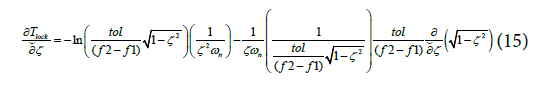
Simplifying Equation (15), one obtains a second expression for the derivative of lock time with respect to the DC,
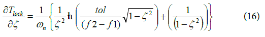
Equation (16) is the derivative of the lock time has two terms. The first term of the derivative is dependent on the frequency step size and the tolerance of frequency deviation. The second term in Equation (16) is a function of the DC. The relationship between natural frequency and loop BW in terms of DC is written as:

By substituting Equation (17) in Equation (16) a new expression for the derivative of Lock time is obtained in terms of loop bandwidth and DC is written as:
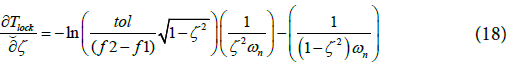
Equation (18), relates the derivative of the lock time with the loop BW with natural frequency and DC. Such an expression (Equation 18) has not been discussed in open literature.
Figure 2 illustrates the variation of the lock time of a second order PLL with change in PM for different values of natural frequency. It is observed that the lock time of a second order PLL drops rapidly as the PM is increased. The second observation is that Lock Time is almost inversely proportional to the natural frequency of the PLL.
The result of Figure 2 tracks generated for a frequency step size of 1 MHz (f2-f1) and a frequency tolerance (tol) of 1 kHz. Banerjee [2] (Equation 16.39) provides the relationship between PM and DC as:

Figure 2: Lock Time vs. PM for Type I second-order PLL for 3 different values of natural frequency (A: 2.6 MHz; B: 5.2 MHz; C:7.8 MHz).
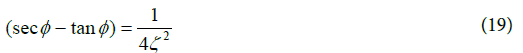
In Equation (19), Φ is the PM of a second-order PLL, and ζ is the DC of a second-order PLL. Taking derivative of both sides of Equation (19) with respect to the PM one obtains:
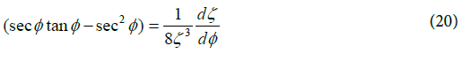
From Equation (20) the derivative of the Lock Time to the PM can be written as:
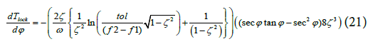
Equation (21) for the derivative of Lock Time with respect to PM has not been derived in open literature. A perturbation of either KV (VCO sensitivity) or capacitance of Loop filter (C) leads to a perturbation of the PM. Perturbation of the Lock Time for a nominal PM value is illustrated in Figure 3.

Figure 3: Perturbation of lock time with nominal PM.
Lock time perturbation vs. PM (Figure 3) was generated for an input frequency step size of 1 MHz and a frequency tolerance of 1 kHz. The X –axis of Figure 3 is the initial PM before perturbation and the Y-axis is the perturbation of the lock time(microseconds). In Figure 3, the lock time is defined as the time required to settle within 1 kHz of the final frequency. The natural frequency of the PLL is fixed at 10 MHz frequency. At PM levels higher than 55o the variation in lock time is lower for a given PM. Equation (22) relating the lock time to tangent of the PM has been derived for the first time.
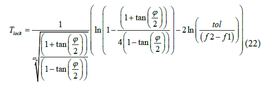
A third expression relates the lock time of a second order PLL to the loop filter time constant. This has not been discussed in open literature and relates lock time to PM as:
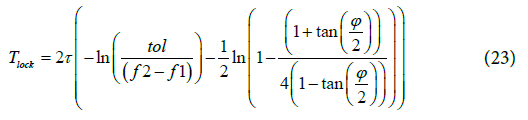
Equation (23) is relates the PLL Lock time to its filter time constant and half of PM.
The relationship between jitter and PM for a Type I and Type II second-order PLL is explored in this section. The derivations in this section originate in [1] and [6]. Type I PLL has been discussed in the previous sections. A brief discussion on Type II PLL in terms of its transfer function is also presented. The Type II PLL of second-order has an additional zero as compared to a Type I second-order PLLs.
The block diagram of Figure 4 illustrates the loop filter, VCO, divider and PFD of a second-order Type II PLL. Transfer function of a Type II PLL is written as:

Figure 4: Type II PLL illustrating loop filter with one pole and one zero.
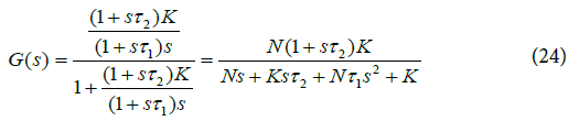
Dividing numerator and denominator of Equation (24) by the transfer function of a Type II PLL can be written as:
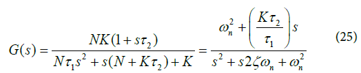
For a Type II PLL the natural frequency is defined as:

The DC for a Type II PLL can be written as:

This section discusses the relationship between Jitter and PM of a Type I and Type II second-order PLL. Type II PLLs have a zero in their transfer function unlike Type I PLLs. Different transfer functions for Type I and Type II PLLs as illustrated in Figure 5.

Figure 5: Difference in TFs of Type I and Type II PLL.
The period jitter variance is related to the phase noise generated by various sources of noise within the PLL through Fourier integral [6].
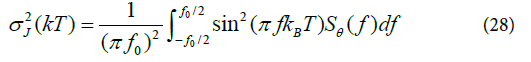
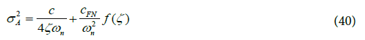
In Equation (28), Sθ ( f ) is the phase noise of a frequency source, f0 is the center frequency, σ 2J (KT) is the variance of period Jitter, kB is the Boltzmann’s constant, and T is the absolute temperature. If Sθ ( f ) is known, Equation (28) facilitates the computation of jitter variance when phase noise is known. Considering only the noise source of VCO, a relationship between Root–Mean-Square (RMS) jitter variance, damping coefficient and natural frequency have been given by Lee [1] for a second-order Type II PLL.
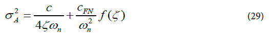
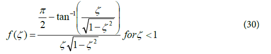
In Equation (29), σ 2A is the Variance of absolute jitter at PLL output (sec2), C WN is the Jitter coefficient for white noise (unit seconds), C FN is the Jitter coefficient for flicker noise (dimensionless) In turn, ωn and ζ is the Damping coefficient of Type II second order PLL. Function f ( ζ ) is the non-linear Flicker noise function. Equation (29) comprises two terms – the first term is the contribution of the white noise and the second term is the contribution of the flicker noise. The flicker noise coefficient is a function of the damping coefficient and PM of the PLL. For an underdamped PLL, the flicker noise coefficient has been described by Lee [1] as:
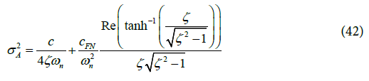
The corresponding expression in Lee [1] for the flicker noise coefficient of an over-damped PLL is
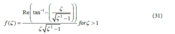
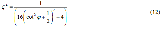
Operator Re in Equation (31) implies only the real part of the hyperbolic inverse is considered. Current paper relates the PM to the jitter variance for a Type II PLL. Rearranging Equation (30) one obtains:
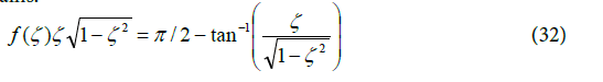
The RHS of Equation (32) is simplified as:

The fourth root of both sides of Equation (12) yields an expression for the DC in terms of PM written as:

Substituting ζ from Equation (34) in Equation (30), the flicker noise function can be written as:
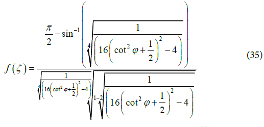
Equation (35) relates the f (ζ) in terms of PM ' Φ ' Substituting Equation (35) into the expression for jitter in Equation (29) one obtains an expression for the jitter variance.
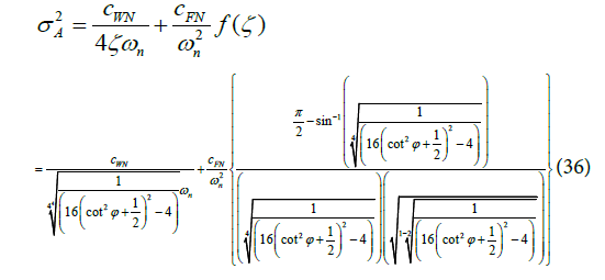
Equation (36) for an underdamped Type II PLL relates the PM and Jitter variance for the first time in open literature.
Alternative relationship between PM and absolute jitter for type II PLL
The relation between PM and absolute jitter for type II PLL can be analytically derived using another procedure. The loop bandwidth (ω c) can be expressed as a function of natural frequency (ω c) [2] as:

Damping coefficient  can be expressed as a ratio of loop BW and natural frequency. From the Equation by Banerjee [2]

Modifying Equation (38) by taking a square root one obtains

An expression for the variance of absolute jitter is written as:
Substituting Equation (39) into Equation (40) a new expression relating the variance of the Jitter with the PM is written as
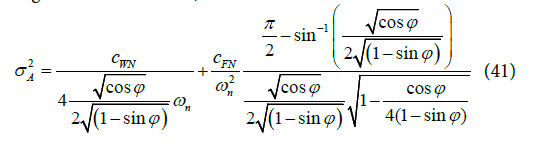
Equation (41) facilitates the determination of the absolute jitter for the under-damped Type II second-order PLL in terms of PM. Such an expression is not expressed in open literature.
For the over-damped Type II second-order PLL, the jitter variance expression (Equation 43) includes a hyperbolic term.
Substituting DC from Equation (40) in Equation (42), the jitter variance is written in terms of the PM as
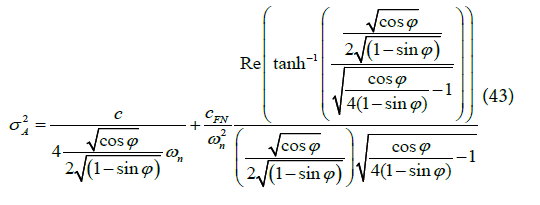
Equation (44) relates the absolute jitter for over-damped Type II second-order PLL in terms of PM. Such an expression is not expressed in open literature. Figure 6 depicts jitter variance vs. PM for various values of ωn.

Figure 6: Jitter Variance vs. Phase Margin for Type II PLL (A: ωn =3.46 × 10⁴ rad/sec; B: ωn =4.9 × 10⁴ rad/sec; C: ωn =6.9 × 10⁴ rad/sec).
Figure 6 illustrates that greater the PM, lower is the jitter variance for Type II PLL. Figure 6 is computed for the values of c=1.67 x10- 17sec; cFN=1.6 × 10⁻¹¹. For the same PM (e.g. 50°), the jitter variance is significantly reduced as ωn is increased. In paper [6] closed-form jitter variance models for type I PLL of second-order PLLs are derived. A noise figure K for the VCO noise source (white) is defined as
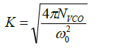
Parameter K2 is the figure of merit of the VCO. In Equation (44), ωo is the center-frequency of VCO, and NVCO is the Phase noise of the VCO, dBc/Hz. In Equation (44), the units of K are 1/ √HZ . The VCO noise term VCO N is a product of two terms, K2 e2n = Hz2/V2 ×V2 /HZ . The unit of the constant K2 (gain of the clock source oscillator) is Hz/V and the unit of the white noise voltage en is volts / √HZ Figure 7 illustrates the change in jitter variance with the change in PM for an underdamped PLL. Jitter variance for Type I second-order under-damped PLL [6],

Figure 7: RMS jitter predicted by Mansuri’s [27] model for under-damped second-order PLL (VCO noise).
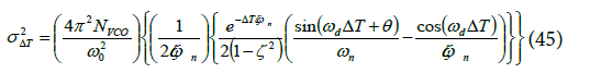
The damped frequency (ωd) is defined as

In turn, the additional phase shift is defined as

Figure 7 illustrates the change in jitter variance with the change in PM for an underdamped PLL.
In Figure 7, the DC ranges from 0.42 to 0.9 with figure of merit 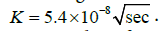 In Figure 7 each value of PM corresponds to a unique value of DC. This value of DC is substituted into the timeinvariant (not a function of part of in Δ T Equation (47) to compute the Jitter variance. Exponential term in Equation (47) goes to zero when interval Δ T goes to infinity. Figure 7 illustrates that the RMS jitter value is reduced from 5 × 10-12 sec2 to 3.2 × 10⁻¹² sec2 as the PM increases from 45o to 75o.To simplify one must consider the function within the brackets in Equation (46) which is the multiplicative part of jitter variance and independent of k.
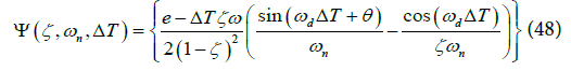
In Equation (48), ΔT is the Time interval under consideration for Jitter measurement.Ψ ( ζ ,ωn ,ΔT ) is the jitter variance function which is dependent only on ΔT,ζ and ωn .
Settling time of a second order PLL is written as:
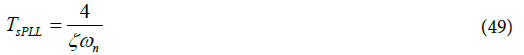
Figure 8 shows the variation of Jitter variance with ΔT , the time interval for jitter variance estimation for various values of PM. The Y axis of Figure 8 is the Jitter variance divided by 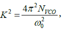 figure of merit of the VCO. After an initial transient, only the steady state part contained in the first term of Equation (45) dominates, this is when ΔT is larger.

Figure 8: Jitter Variance function vs. ΔT for 3 values of PM for secondorder under damped PLL.
Figure 8 illustrates that the component which is a function of time interval ΔT ωn and ζ , damping coefficient exhibits oscillatory behavior and settles down to a final value within ΔT =2 × 10⁻⁷. Higher the PM lower is the final value of jitter variance and lower the initial high part of the jitter variance. Figure 8 is illustrated for 3 values of PM for and under-damped PLL. When PM is varied between 42° and 66°, the initial peak reduces from 26 × 10-8 to 1.2 × 10⁻⁸. Figure 9 illustrates the jitter variance function in [6] vs. PM for a fixed value of ΔT for second-order Type I PLL

Figure 9: Jitter Variance function for fixed ΔT vs. PM.
Figure 9 illustrates that Jitter variance σ2ΔT for the PLL is reduced as the PM is increased. Figure 10 illustrates the variation of the Jitter variance function with settling time of a second-order PLL.

Figure 10: Jitter variance function ( Ψ ζ ,ωn ,ΔT ) vs. settling time of a second-order type I PLL.
Figure 10 illustrates that the jitter variance function increases with increased settling time (lower DC).
A plot of the jitter variance vs. PM for the over-damped PLL is illustrated in Figure 11.

Figure 11: Jitter variance vs. phase margin.
Figure 11 illustrates that the higher value of PM reduces the value of jitter variance of a second-order overdamped PLL.
Jitter Variance vs. PM of a II Order PLL
An analytical contribution in the form of an extension to models described in [27] has been presented in this section.
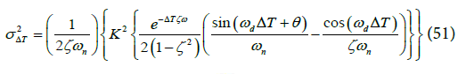
Analytical relationship between the PM (Φ ) and the periodic jitter of PLL is given in Equation (51).
Substituting DC in the jitter variance expression of [6] for underdamped PLLs in Equation (51),
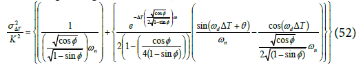
Excluding the figure-of-merit k2 the variance can be written as
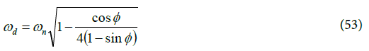
Damped frequency is defined in terms of (ωn) and PM as
Equation (53) is new and relating jitter to PM. An expression for the derivative of jitter variance with respect to the PM of a secondorder PLL is derived here. The first term is the derivative of the first additive term of the RHS of Equation (52),
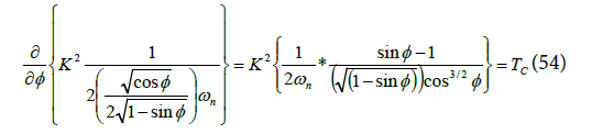
The second term is the derivative of the exponential term of the second additive term in Equation (52) excluding the common factor K2,
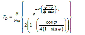
Equals
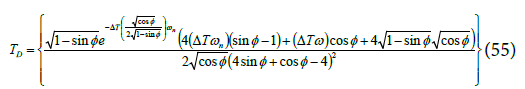
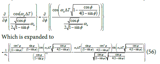
The third term is the derivative of the sinusoidal term of the second additive term in Equation (54). Substituting.  and the additional phase shift angle.
The final substitution is 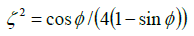
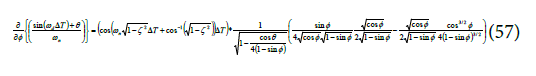
The combined expression for the derivative of Jitter variance with respect to phase margin is written as
Equation (58) is an original contribution of this paper. A derivative of the Jitter variance with respect to PM is not reported in open literature. It is useful for optimization techniques such as Lagrange multipliers applied to a PLL.
Conclusion
New equations have been derived for the variation of Lock time with PM. Lock time and perturbation of Lock time vs. PM has been characterized for the first time in a detailed way. Lock time has been related to half of phase margin for the first time in a closed form expression.
New equations have been derived for jitter variance in terms of PM and DC based on Lee’s [1] model for Type II PLLs [1]. Using Lee [1] closed for equations, Jitter variance has been characterized in closed form for both underdamped and overdamped PLLs.
For the first time equations relating Jitter variance with PM for the closed for expressions due to Mansuri [8] have been derived. Mansuris [27] equations have been extended to cover jitter variance as a function of PM. New curves have been published for Jitter variance vs. time interval for the first time. New equations have been derivd for the variation of DC with PM.
References
- Lee D (2002) Analysis of jitter in phase-locked loops. IEEE Trans Circuits Syst II: 40: 704-712.
- Banerjee D (2007) PLL performance, simulation and design. Dog Ear Publishers, USA.
- Daniels B, Farrell R (2008) Non-linear analysis of the 2nd order digital phase locked loop. IET Irish Signals and Systems Conference, Galway, Ireland.
- Amornthipparat A, Rangsiwatakapong A, Eungdamrong D (2008) Simulation of mathematical phase noise model for a phase- locked-loop. Thammasat University.
- Daniels B (2008) Analysis and design of high order digital phase locked loops. National University of Ireland.
- Drucker E (2000) Model PLL phase noise and performance. Microwaves and RF 2000: 73-82.
- He X (2007) Low phase noise CMOS PLL frequency synthesizer. University of Maryland.
- Savic M, Nicolic M, Milovanovic D (2007) Frequency synthesizer design. CMOS, Proc. 51st ETRAN Conference, Igalo.
- Razavi B (1998) RF Microelectronics. Pearson Education, New Jersey.
- Golestan S, Monfared M, Freijedo FD, Guerrero JM (2013) Dynamics assessment of advanced single-phase PLL structures. IEEE Trans Ind Electron 60: 2167-2177.
- Herzel F, Piz M (2005) System-level simulation of a noisy phase-locked loop. European Gallium Arsenide and Other Semiconductor Application Symposium, Paris.
- Herzel F, Osmany F, Schyett C (2010) Analytical phase noise modeling and charge pump optimization for fractional-N PLLs. IEEE Trans Circuits Syst-I 57: 1914-1924.
- Hangmann C, Hedayat C, Hilleringmann U (2014) Stability analysis of a charge pump phase-locked loop using autonomous difference equations. IEEE Trans Circuits Systems I 61: 104-120.
- Hangmann C, Hedayat C, Hilleringmann U (2013) Enhanced event-driven modeling of a CP-PLL with nonlinearities and nonidealities. IEEE 56th International Midwest Symposium on circuits and Systems, Columbus.
- Gardner F (1980) Charge-pump phase-lock loops. IEEE Trans Commun 28: 1849-1858.
- Van Paemel M (1994) Analysis of a charge-pump PLL: A new model. IEEE Trans Communs 42: 2490-2498.
- Carlosena A, Lazaro A (2007) Design of high order phase-lock loops. IEEE Trans CAS-II 54: 9.
- Hedayat CD, Hachem A, Leduc Y (1999) Modeling and characterization of the 3rd order charge-pump PLL: a fully event-driven approach. Analog Integrated Circuits and Signal Processing 19: 25-45.
- Wang K (2010) Spur reduction techniques for fractional N PLLs. University of California San Diego.
- Abramowitz DY (1988) Analysis and design of a third-order phase locked loop. Military Communications Conference, San Diego.
- Monteiro L, Filho D, Piquiria J (2004) Bifurcation analysis of third-order phase locked loops. IEEE Signal Proc Letters 11: 494-496
- Abdelfattah O, Shih I, Roberts G (2013) Analytical comparison between passive loop filter topologies for frequency synthesizer PLLs. In IEEE 11th International New Circuits and Systems Conference (NEWCAS), Paris.
- De Almeida MO, Santos ET, Araújo JM (2014) Improved performance phase detector for multiplicative second-order PLL systems using deformed algebra. J Circuits Systems Comput 23: 1417-1421.
- Kim DS, Song H, Kim T, Kim S, Jeong DK (2010) A 0.3–1.4 GHz all-digital fractional-N PLL with adaptive loop gain controller. IEEE J Solid-State Circuits 45: 2300-2311.
- Weigand C, Hangmann C, Hedayat C, Hilleringmann U (2011) Modeling and simulation of arbitrary ordered nonlinear charge-pump phase-locked loops. Semiconductor Conference, Dresden.
- Dorf R (2005) Modern control systems. Pearson Publishers, London.
- Mansuri M, Ken CK (2002) Jitter optimization based on phase-locked loop design parameters. IEEE J Solid-State Circuits 37: 1375–82.