Spanish
  Chinese
  Russian
  German
  French
  Japanese
  Portuguese
  Hindi
Hindi Research Article, J Electr Eng Electron Technol Vol: 7 Issue: 2
Study and Analysis of Flyback with Adding RC and CatchWinding Forward DC-DC Power Converter in CCM and DCM
Mamdouh L Alghaythi* and Naz E Islam*
Department of Electrical and Computer Engineering, University of Missouri College of Engineering, University of Missouri, Columbia, USA
*Corresponding Authors : Mamdouh L. Alghaythi
Department of Electrical and Computer Engineering, University of Missouri Columbia College of Engineering, Columbia-65211, USA
Tel: + (1-618) 3055095
E-mail: mlagzd@mail.missouri.edu
Naz E. Islam
Department of Electrical and Computer Engineering, University of Missouri Columbia-65211, USA
E-mail: islamn@missouri.edu
Received: June 06, 2018 Accepted: June 25, 2018 Published: June 30, 2018
Citation: ML Alghaythi, NE Islam (2018) Study and Analysis of Flyback with Adding RC and Catch-Winding Forward DC-DC Power Converter in CCM and DCM. J Electr Eng Electron Technol 7:2. doi: 10.4172/2325-9833.1000159
Abstract
The isolated DC-DC converters are completely separated between the input and the output terminals. However, the non-isolated DC-DC converters would share a common ground between the input and the output terminals. The isolated DC-DC converters can be used as a positive grounding or negative grounding. Furthermore, isolated converters have found wide application recently due to their advantage over non-isolated converters. In addition, electrical isolation of input and output ground connections is for safety. The voltage and current stress on switches can be minimized using transformers. Moreover, the first winding can be used to put in energy into the inductor; as a result, the inductor that could gradually increase the energy from the inductor to the load cannot be available for the other coil. The two significant topologies of the isolated DC-DC converters are flyback converter and catch-winding forward converter. Therefore, the main goal is to analyze and investigate the impact of change in switching frequency, duty ratio, load and the input voltage for every topology and to find the critical points for every topology by comparing the results with every figure done through this work [1].
Keywords: Flyback converter; Catch-winding forward converter; DC-DC converter
Introduction
The isolated DC-DC converters are completely separated between the input and the output terminals. However, the non-isolated DCDC converters would share a common ground between the input and the output terminals. The isolated DC-DC converters can be used as a positive grounding or negative grounding. Furthermore, isolated converters have found wide application recently due to their advantage over non-isolated converters. In addition, electrical isolation of input and output ground connections is for safety. The voltage and current stress on switches can be minimized using transformers. Moreover, the first winding can be used to put in energy into the inductor; as a result, the inductor that could gradually increase the energy from the inductor to the load cannot be available for the other coil. The two significant topologies of the isolated DC-DC converters are flyback converter and catch-winding forward converter. Therefore, the main goal is to analyze and investigate the impact of change in switching frequency, duty ratio, load and the input voltage for every topology and to find the critical points for every topology by comparing the results with every figure done through this work [1].
Flyback Converter
First of all, flyback converter is an isolated converter, which is designed based on a buck- boost converter by using a coupled inductor. In addition, by changing the inductor of the buck- boost to flyback transformer, it would clearly be a lucid model of flyback converter. Furthermore, the primary transformer has been connected in series with the input voltage and switch; a complete model with a magnetizing inductance and has been shown in Figure 1. Moreover, it is important to know that losses and leakage inductance would clearly affect the switch performance. Flyback converter has two modes of operation in CCM; one is charging magnetizing inductance and the other is discharging magnetizing inductance load into the load. On the other hand, when flyback is in DCM, it will have three modes of operation; first is charging magnetizing inductance, second is discharging magnetizing inductance and third mode is when transformer is off. Basically, as it turns out, the diode and switch used here are ideal, also the voltages and currents are totally periodic besides having a huge output capacitor as the secondary of the flyback transformer [2].

Figure 1: Flyback converter with adding RC instead of zener diode.
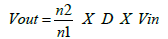
Theoretically a relation exist between the output voltage and input voltage of a flyback converter in continuous conduction mode as shown in equation 1
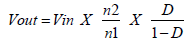 (1)
(1)
For the discontinuous conduction mode, the relation can theoretically be expressed as in equation 2
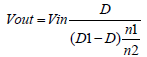 (2)
(2)
Impact of change in switching frequency
The circuit has essentially to be set at its nominal duty ratio, switching frequency and load in order to observe the impacts of changing switching frequency. Therefore, (D=20%, F=10 KHZ and R=80 Ω). Moreover, channel 1 shows the MOSFET drain voltage, channel 2 shows the current in the primary of coupled inductor, channel 3 shows the voltage on the secondary of the coupled inductor and channel 4 shows the output voltage as shown in Figure 2. On the other hand, the current in the primary of the inductor can theoretically be calculated as in equation 3

Figure 2: Simulation with nominal operating points F=10 KHZ, D=20%, 500 mA/dIV.
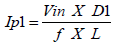 (3)
(3)
From Figure 2, it can be observed the MOSFET drain voltage=43.6V on channel 1, the primary current I peak=0.46 A on channel 2 and Vsw= -33.6 V on channel 3 and Vout=8.6 V on channel 4. As it is shown above in Figure 2, the voltage on the secondary is in DCM mode. However, as switching frequency increases, the converter would essentially enter the continuous conduction mode (CCM).
Furthermore, with an input voltage of 12 V, duty ratio adjusted to be 36.6% in order to get an output voltage of 15 V, Ip1 is 0.69 A as it is shown in equation 4, MOSFET drain voltage is 45.2 V and voltage on the secondary is -28.8 V as shown in Figure 3.

Figure 3: Simulation with nominal operating points D=36.6%, 500 mA/dIV.
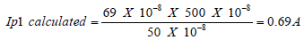 (4)
(4)
As switching frequency is increased to 20 KHZ, duty ratio (D) is set to be 47.7% to keep output voltage constant and Ip1 is 0.6 A shown in Figure 4.

Figure 4: Simulation with nominal operating points F=20 KHZ, D=47.7%, 500 mA/dIV.
From the waveforms above ILMmax around 75 A and ILMmin around 38 A, diode current ID1 max around 15 A and ID1 min is zero, for capacitor current ICmax around 7.8 A but ID1min around -7.8 in the negative as shown in Figure 5.

Figure 5: Magnetizing inductance current, diode current, and capacitor current waveforms vs. time.
In addition, when switching frequency is increased to 30 KHZ, D is set to be 50.6% and Ip1 is 0.48 A as shown in Figure 6.

Figure 6: Simulation with nominal operating points F=30 KHZ, D=50.6%, 500 mA/dIV.
Also, when switching frequency is increased to 40 KHZ, D is set to be 52.4% and Ip1 is 0.42 A as shown in Figure 7. Thus, it can be observed from increasing switching frequency that the converter enters the continuous conduction mode and the current in the primary decreases. It is noticed that the current in the primary is the current ripple in the primary inductance. However, the reason behind existence of the voltage spikes on flyback might be the leakage inductance around primary winding, or it might be a mistake happened when transformer was wounded. In order to reduce the high voltage spikes, RCD snubber should add in parallel with primary winding or increase the primary inductance as shown in Figure 6.

Figure 7: Simulation with nominal operating points F=40 KHZ, D=52.4%, 500 mA/dIV.
Thus, the critical point is when f=87.8 KHZ, the converter is in CCM, which is specified by the blue hexagon shown in Figure 8. Furthermore, when f=87.8 KHZ, D=75.2% and Ip1=0.44 A shown below. In this work, some difficulties happened through this experiment in terms of burning of two zeners. However, despite of facing some difficulties, it has become a must to replace the burning zeners by the following parameters; (parallel resistances 330 Ω, 50 Ω and capacitor of (0.1 μF) in order to avoid the burning Zener diode again.

Figure 8: Critical point at F=87.8 KHZ, D=75.2% , 500 mA/dIV.
To compare the critical point with the relation between the output voltage and input voltage, it is a must to use equation 1.
(1)
D is calculated to be 52.4%, Vin is 12 V, n2:n1 is 2:1, as a result, Vout is 26 V. Even though the expected output voltage is 15 V, the calculated output voltage is 26 V, which essentially means that the reason would be the losses in the switches and other components; such as calculating the duty ratio which is not always accurate.
Impact of changing the load
Changing the load plays a remarkable role and in order to realize this effect, the circuit has to set at its nominal condition in CCM. With a switching frequency=40 KHZ, D=56.6% and R decreased to be 60 Ω. When R=60 Ω, D=56.6% and Ip=0.5 A as shown in Figure 9.

Figure 9: Simulation with nominal operating points F=40 KHZ, R=60 Ω, D=56.6%, 500 mA/dIV.
When R decreased to 40 Ω, some difficulties happened through experiment, such as burning of two zeners. However, despite facing some difficulties, it has become a must to replace the burning zeners and try again. As a result, when R=40 Ω, then D=68% and Ip1=0.68 A as shown in Figure 10. Thus, it can be observed that once the load increased (load resistance decreased), the current in the primary of inductor (I peak) completely increased. In addition, in order to keep output voltage constant, duty ratio has to be large.

Figure 10: Simulation with nominal operating points R=40 Ω, D=68%.
Impact of decreasing the input voltage
Switching frequency is set to 40 KHZ, Vin to 12 V, but in order to observe the effect, the input voltage has to decrease to 9 V. When Vin decreases to 9V duty ratio increases to 73.4% and Ip1 decreases to 0.5 A. Consequently, when input voltage decreased, the peak current in the primary of the inductor decreased, but the duty ratio increased to keep the output voltage constant. As soon as the input voltage decreased, the output voltage increased.
Furthermore, the flyback transformer input voltage is less than the source voltage and the reason behind that is the switching and resistive voltage drops in the circuit.
Catch-Winding Forward Converter
Catch-winding forward converter is designed based on isolating a buck converter as shown in Figure 11. The main purpose of using transformer here is to increase and decrease the output voltage. However, the only difference between buck converter and forward converter in terms of the voltage across diode is the ratio n2:n1 or the magnitude of the voltage. That means that the maximum output voltage is basically constrained by turns ratio. Therefore, the relation between the input voltage and the output voltage is:

Figure 11: Simulation with nominal operating points F=40 KHZ, D=73.4%, 500 mA/dIV.
 (5)
(5)
The transformers in the catch-winding cannot store energy, which means that energy will directly pass to the output of forward converter [3]. The diodes used here are 1N5819 (Figure 12).

Figure 12: Catch-winding forward Converter 1:0.5:3.
Impact of changing switching frequency
First of all, the purpose here is to observe the effect of the changing switching frequency on the peak MOSFET current and the output voltage. However, the circuit generally has to be set at its nominal frequency, duty ratio and load (D=33%, F=20 KHZ and R=12 Ω) to keep the output voltage at 12V. For Figure 13, channel 1 shows the MOSFET drain voltage, channel 2 shows the current in the MOSFET, channel 3 shows Q (t) and channel 4 shows the output voltage. When f=20 KHZ, the peak drain voltage=48.8V on ch.1, the peak MOSFET current Ip = 0.66 A on channel 2 and the high plateau drain voltage=34.8 V as shown in Figure 13.

Figure 13: Simulation with nominal operating points F=21.8 KHZ, D=33%, R=12 Ω, 500 mA/DIV.
Duty ratio adjusted to 43.2% until the output voltage is 12 V, Vin=12 V, so the peak drain voltage=49.6 V, the peak MOSFET current Ip = 0.85 A and the high plateau drain voltage = 34.8 V as shown in Figure 14.

Figure 14: Simulation with nominal operating points F=21.8 KHZ, D=43.2%, 500 mA/DIV.
When D=45.2%, MOSFET on time=10.8 μs, the peak MOSFET current Ip=0.88 A, the time that the catch winding diode is conducting=21 μs and peak drain voltage=75.2 V and the high plateau drain voltage=34.8 V shown in Figure 15.

Figure 15: Simulation with nominal operating points F=20 KHZ, D=45.2%, 500 mA/DIV.
As mentioned earlier in order to avoid or lower the high voltage spikes, RCD snubber should be add in parallel with primary winding or increase the primary inductance as shown in Figure 15.
On the other hand, when switching frequency=30 KHZ, Duty ratio=44.6% to keep output voltage constant and the peak current Ip=0.80 A shown in Figure 16.

Figure 16: Simulation with nominal operating points F=30 KHZ, D=44.6%, 500 mA/dIV.
In addition, for Figure 17, switching frequency is increased to 40KHZ, then Duty ratio=45.8% and the peak current Ip=0.76 A [4].

Figure 17: Simulation with nominal operating points F=40 KHZ, D=45.8%, 500 mA/dIV.
However, since the forward converter is generally an isolated buck converter, the formula of the inductor current ripple can be used here as in equation 6:
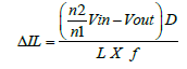 (6)
(6)
From the waveforms and relation above, it can observe that increasing the switching frequency will decrease the inductor current ripple and therefore, output ripple voltage will decrease too. Moreover, from the waveforms above as switching frequency increases, the peak MOSFET current decreases [5,6].
Impact of changing the load
Changing the load would essentially affect the parameters in the converter. So in order to realize this effect, the circuit has to set at its nominal f=20 KHZ, D=33% and R=24 Ω, Ip=0.56 A, then increased to 48 Ω, after that resistance is increased until the converter is in DCM (the critical point of operation) R=72 Ω. For Figure 18, at R=24 Ω, duty ratio adjusted to 39%, Ip1=0.56A and for Figure 19, resistance increased to 48 Ω, duty ratio adjusted 36%, Ip1=0.40 A. However, resistance increased until the converter is in DCM (the critical point of operation happened when R=72 Ω) and duty ratio=45% and Ip1=0.41 A.

Figure 18: Simulation with nominal operating points R=24 Ω, D=39%, Ip1=0.56 A.

Figure 19: Simulation with nominal operating points R=48 Ω, D=36%, Ip1=0.40 A.
The trailing edge of the MOSFET drain voltage has been specified by the violet hexagon above in Figure 20, which means the converter is going to be in DCM. Thus, it can be observed that decreasing load (increasing the load resistance) can make the circuit in discontinuous conduction mode. Since catch-winding forward converter is an isolated buck converter, it can be observed that increasing resistance (which decreases load) would increase the output voltage and output voltage ripple. However, that would essentially decrease the inductor current, with a reduction in the inductor current ripple then increasing in the output voltage [7].

Figure 20: Critical point when R=72 Ω, D=45%.
Impact of changing the output voltage
The circuit is set at its nominal (f=20 KHZ, D=33%, Vin=12 V, R=12 Ω). Figure 21 shows that when Vout=15 V, duty ratio D=58.6%, the peak drain voltage=50 V, the peak MOSFET current=1.06 A and the high plateau drain voltage=59.6 V.

Figure 21: Simulation with nominal operating points Vout=15 V, D=58.6%.
However, to notice the effect of the output voltage, it is a must to look back the value of the duty ratio at the nominal conditions. When the duty ratio was 33%, it basically showed that once the duty ratio increased, the output voltage essentially increased and therefore the peak drain Voltage and the peak MOSFET current are increased as it has already been mentioned before that the relation between the input voltage and the output voltage . In addition, equation 5 would truly help out since the output voltage is directly proportional to the input voltage. As the output voltage increases, the duty ratio and the input voltage will increase; the best example to investigate this relation is at the lab when the output voltage increased from 9 V to 15 V, duty ratio completely increased,
(5)
As mentioned earlier the voltage on the secondary is a pulsed waveform, but the output voltage in forward converter is buck converter. That means the effect of the output voltage on forward converter would essentially be the same for the buck converter.
The linearity between the output voltage, switch duty ratio is lost, which generally means that the output voltage controller circuit will not be able to maintain the required quality of the output voltage [8-10].
Conclusion
Two significant isolated DC-DC converters were analyzed through this work. Furthermore, the impact of changing switching frequency, duty ratio, load and the input voltage is studied for flyback and catch-winding forward converter. On the other hand, some equations have been provided to observe and compare the results with the figures. Moreover, the critical point between CCM and DCM has been illustrated in the figures. Once switching frequency increases, the peak current and the output voltage decreases in the flyback converter. Also, that would decrease the MOSFET drain voltage, the current in the MOSFET and the output voltage in the catch- winding converter. As a result, the duty ratio has gradually been increased to keep the output voltage constant for the flyback and catch-winding forward converter. Based on that when the duty ratio increased, the output voltage increased. However, the calculated theoretical value of the output is not completely the same for the duty ratio and the input voltage and the reason behind that would essentially be the losses in the converter. On the other hand, increasing switching frequency would make the converter enter the continuous conduction mode and decreases the current in the primary, after that finding the critical point would be easy as it is explored in Figure 7. Once the load increased (load resistance decreased) in flyback converter, the current in the primary of inductor (I peak) completely increased and decreases the output voltage. However, for the catch-winding forward converter, when the load increased (load resistance decreased) can make the circuit in discontinuous conduction mode; the critical point is explored in Figure 19. Consequently, feedback loop is a remarkable way to set the duty ratio for maintaining the right output voltage.
References
- Daniel WH (1996) Introduction to Power Electronics. Prentice Hall Inc.
- Dixon LH (1996) Filter Inductor and Flyback Transformer Design for Switching Power Supplies. Unitrode Power Supply Design Seminar Manual SEM-1100, Lexington.
- Jovanovic MM, Zhang MT, Lee FC (1995) Evaluation of synchronous-rectification efficiency improvement limits in forward converters. IEEE Trans Ind Electron 42: 387-395.
- Cascio JL, Nalbant M (1990) Active Power Factor Correction Using a Flyback Topology. PCIM conference, Munich.
- Andreycak W (1999) Practical Considerations in High Performance MOSFET, IGBT and MCT Gate Drive Circuits, Unitrode Application Note U-137. Texas Instruments Incorporated.
- Billings KH (1989) Handbook of Switch mode Power Supplies. McGraw-Hill.
- Karvelis GA, Manolarou MD, Malatestas P, Manias SN (2001) Analysis and design of non dissipative active clamp for forward converters. IEE Elect Power Applicat 148: 419-424.
- McGarry L (2004) The standby power challenge. 2004 International IEEE Conference on the Asian Green Electronics, Hong Kong and Shenzhen.
- Spiazzi G, Tagliavia D, Spampinato S (2000) DC-DC flyback converters inthe critical conduction mode: A re-examination. IEEE IA Annual Meeting 4:2426–2432.
- Lidak P (1998) Critical conduction mode flyback switching power supply usingthe MC33364. Motorola Semiconductor Application Note (AN 1594D).