Spanish
  Chinese
  Russian
  German
  French
  Japanese
  Portuguese
  Hindi
Hindi Research Article, J Nucl Ene Sci Power Generat Technol Vol: 11 Issue: 6
The Dependence of Charge Carriers on the Methods of Thermal Processing of Residence Time on Silicon, Legalized with Copper and Iridium
AK Rafikov1*, SH A Maxmudov1, AA Sulaymonov1 and JZ Mirzarayimov2
1Department of Physics, Institute of Nuclear Physics of the Academy of Sciences of the Republic of Uzbekistan, Tashkent, Uzbekistan
2Department of Engineering and Technology, Namangan Institute of Engineering and Technology, Namangan, Uzbekistan
*Corresponding Author: AK Rafikov
Department of Physics,
Institute of
Nuclear Physics of the Academy of Sciences of the Republic of Uzbekistan,
Tashkent,
Uzbekistan;
E-mail: rafikov@inp.uz
Received date: 07 April, 2022, Manuscript No. JNPGT-22-59957; Editor assigned date: 11 April, 2022, PreQC No. JNPGT-22-59957 (PQ); Reviewed date: 25 April, 2022, QC No. JNPGT-22-59957; Revised date: 06 June, 2022, Manuscript No. JNPGT-22-59957 (R); Published date: 13 June, 2022, DOI: 10.4172/2325-9809.1000294
Citation: Rafikov AK, Maxmudov SHA, Sulaymonov AA, Mirzarayimov JZ (2022) The Dependence of Charge Carriers on the Methods of Thermal Processing of Residence Time on Silicon, Legalized with Copper and Iridium. J Nucl Ene Sci Power Generat Technol 11:6.
Abstract
In this work, we investigated the dependence of the concentration of centers of energy levels on the lifetime of charge carriers in silicon samples doped with copper and iridium, and the electrophysical, photoelectric and recombination properties of the sample under the influence of thermal and radiation exposure.
Keywords: γ- radiation, Charge life time, Temperature, Energy
level, Copper, Iridium, Chemical, Quasi-chemistry, Fermi level,
Cooling rate
Introduction
The recombination properties of silicon, which has thermal, radioactive, and mixed defects that form deep energy levels (CHES), have been studied in many experimental and theoretical researches [1-4]. The results of some studies show that in n-type silicon, the compensatory forming defect leads to a decrease in the lifetime τ of non-basic charge carriers with increasing concentration of defective center. However, in studies, it was observed that τ increases with increasing concentration of silicon-forming centers [5-10]. In particular, the increase in τ in silicon is explained differently by various authors. For example, in [11-14] the increase in τ is explained by a decrease in the concentration of recombination centers in thermal and radiation treatment, while in the literature the formation of oxygen complexes with various defects is observed. In studies, the increase in τ is explained by the formation of sticky surfaces of the charge carriers and an increase in the degree of non-homogeneity of the conductivity in the process of compensating the silicon charge carriers as a result of external influences.
In silicon doped with copper, acceptor centers with deep surface energies E1=ES-(0.15-0.21) eV, E2 =ES-(0.2-0.49) eV, E3=EV+0.23 eV and donor centers with E4=EV+(0.16–0.21) eV and centers with energy E1=ES-(0.15–0.21) and Es-0.49 eV were strongly correlated with the oxygen concentration in the sample. It was found that an increase in oxygen concentration of ~ 2 order leads to a 2-3-fold increase in the center concentration of E1=Es-(0.15-0.21), and a 3-4-fold decrease in the center concentration in the center with an energy of Es - 0.49 eV. In the slowly cooled n-Si <Cu> samples, deep copper-forming surfaces were observed. It has been studied in the study that the charge carrier’s τ depends on the concentration of copper centers in n-type silicon. The energy of the deep layers formed by silicon doped with iridium is E1=ES-(0.18 ± 0.02); Acceptors with E3=ES-(0.54 ± 0.02) eV and donor centers with E2=ES-(0.32 ± 0.02) eV were identified. No dependence of iridium centers on oxygen concentration was observed. It was observed that the concentration of centers in slow cooled samples was 1.5 times higher than the concentration of fast cooled samples. The dependence of τ on the concentration of iridium centers of n-type silicon has been studied.
From the above, it can be concluded that there are currently no single theoretical views that explain the changing nature of the life times of non-basic charge carriers in silicon. The electrophysical, photoelectric and recombination properties of the sample under the influence of thermal and radiation were studied as the dependence of the concentrations of the energy transfer center on the life of the charge carriers in samples of silicon doped with copper and iridium.
Materials and Methods
Samples of n-type and p-type single crystal silicon (grown by the Chokhralsky method and in a crucible-free zonal solvent) with initial specific resistances of 3–10 Ohm ∙ cm were obtained. In this paper, the hall coefficient method determined the specific resistance, mobility, concentration of the samples, and the lifetime of the charge carriers by the stationary photoconductivity method. Copper and iridium inserts were introduced by vacuum dusting and high temperature diffusion using VUP-4 equipment. For the measurement of deep energy levels, the DLTS operating on a Schottky diode used the nonstationary capacitance spectroscopy method.
Sample preparation
Samples with n- and p-type silicon and pre-irradiated samples with a specific resistance of ~ 3 ÷ 10 Ohm ∙ cm were used as the initial sample. Alloying of silicon with copper and iridium was carried out at 1050-1150°C and then cooled at 30-40 grad/min (type I) and 250-300 grad/min (type II). Simples n-Si<P> and р-Si<B> heat-treated without the same copper and iridium mixture and n-Si<P,P> and p-Si<В,P> previously doped with neutrons, were tested in parallel. In n-Si and r- Si, the ohmic contacts were welded by heating the alloy SN+In (50% +50%) to ~ 120°C, while the Schottky diodes were prepared by vacuum dusting silver Ag and tin Sb on a silicon surface using a VUP-4 device.
Results and Discussion
The results from the study of the effect of copper and iridium on the lifetime of non-basic charge carriers in silicon type I (fast cooled, 250 grad/min) and type II (slow cooled, 30 grad/min) are presented in Tables 1 and 2. In Table 1, it was found that the lifetime of the charge carriers was significantly increased when heated to 1120°C to doped with neutron and controlled n-type I-type silicon (n-Si<P,P> and n- Si<P>). It was found that the lifetime of charge carriers in n-Si<P, P,Cu> samples was 10 times longer than in n-Si<P>, n-Si<P,P> and n- Si<P,Cu>. When normal and to silicon doped with neutron when entered with iridium at temperatures of 1050°C, 1100°C, 1150°C (n- Si<P,Ir>, n-Si<P,P,Ir>), the lifetimes of the charge carriers in them were almost indistinguishable. It was found that the lifetime of charged carriers on n-Si<P,P,Cu> increased 10 times comparing with n-Si<P>, n-Si<P,P>.
| Type samples | Тdif.= 1120°С | Тdif.= 1170°С | ||
|---|---|---|---|---|
| I type τ, сек. |
II type τ, сек. |
I type τ, сек. |
II type τ, сек. |
|
| n-Si<P> | 1·10-6 | 5,4·10-7 | 7·10-7 | 4,3·10-7 |
| n-Si<P,P> | 3·10-6 | 2,4·10-7 | 3.7·10-7 | 2,3·10-7 |
| n-Si<P,Cu> | 1,6·10-6 | 3,8·10-6 | 5,3·10-6 | 4,6·10-6 |
| n-Si<P,P,Cu> | 2,8·10-6 | 5,1·10-6 | 7,2·10-6 | 7,8·10-6 |
| n-Si<P,Ir> | 4,7·10-5 | 6,7·10-5 | 7,6·10-5 | 8,8·10-5 |
Table 1: Non-basic charge carriers in type I and II n-type alloys silicon doped with copper and iridium.
In Table 2, it is detected that the lifetime of the charge carriers was significantly increased when the doped with neutron and controlled ptype I and II (n-Si<P,P> and n-Si<P>) silicon samples were heated to 1100°C and 1150°C. It was found that the lifetime of charge carriers in p-Si<B,P,Cu> samples increased by ⁓ 10 times compared to p-Si<B>,p-Si<B,P> and p-Si<B,Cu>. When ordinary and silicon doped with neutron was doped with iridium at temperatures of 1050°C, 1100°C, 1150°C (p-Si<B,Ir>, p-Si<B,P,Ir>), the lifetime of the charge carriers in them was almost the same, but It was found that the lifetime of the relatively charged carriers heated by p-Si<B,P> and p-Si<B> increased ⁓ 100 times.
| Type samples | Тdif.= 1100°С | Тdif.= 1150°С | ||
|---|---|---|---|---|
| I type τ, сек. |
II type τ, сек. |
I type τ, сек. |
II type τ, сек. |
|
| p-Si<P> | 1,18·10-6 | 1,3·10-6 | 10-Jun | 1,6·10-6 |
| p-Si<B,P> | 1,3.10-6 | 1,6·10-7 | 1,7·10-6 | 2.3·10-6 |
| p-Si<B,Cu> | 3·10-6 | 3·10-6 | 4,8·10-6 | 4,7·10-6 |
| p-Si<B,P,Cu> | 6,4·10-6 | 6,2·10-6 | 7,6·10-6 | 8,8·10-6 |
| p-Si<B,Ir> | 4,2·10-5 | 5,8·10-5 | 6.6·10-5 | 8.8·10-5 |
| p-Si<B,P,Ir> | 4,8·10-5 | 6,2·10-5 | 7.2·10-5 | 9.3·10-5 |
Table 2: Primary non-charge carriers residence times in p-type Silicon samples of type I and II legalized by copper and Iridium.
The results obtained for the doped sample silicon with doped I-type and n-type pre-neutrons were almost indistinguishable, i.e., τ was not observed to depend on the concentration of copper and iridium centers. An insignificant increase in τ was found to be due to an increase in the concentration of Thermo-Defects (TD) in silicon.
The difference in the values of τ in the doped type I and type II samples was explained by the decrease in the concentration of TD. To prove this, doped and previously silicon doped with neutron was heated isochronically at 120–700°C (heating duration ~ 20 min.) and then cooled at a rate of 20 grad/min. It was observed that the residence time of non-basic charge carriers by isochron heating of n-type silicon samples previously silicon doped with neutron under the same conditions with the doped sample depended on the cooling rate (Figure 1). The increase in τ in this case may be related to the decay of the recombination centers formed by the controlled and uncontrolled compounds in the study of silicon.

Figure 1: n-type silicon samples depend on the cooling rate of nonbasic charge carrier’s residence time by isochron heating.
• n-Si <P, R> NDS;
• Silicon doped with copper n-Si<R,Cu>;
• n-Si<P,R,Cu> is preceded by a copper introduction to a silicon doped with neutron;
• n-Si<P,R,Ir> temperature dependence of the lifetime of non-basic charge carriers when iridium is introduced into a previously silicon doped with neutron.
Experiments were performed in 3 different ways to explain the mechanisms of τ increase in doped samples.
When the permeability of the doped material is not homogeneous, τ is determined by the following formula
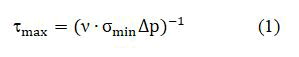
Here σmin is the minimum cross section of the charge carriers on the localized layers: τmin ≥ 10-22 ÷ 10-23 см-2, Δp-change in the concentration of the pits: Δp<5∙1014 см-3, the thermal velocity of the ν- pits: ν ~ 107 cm/s.
The conductivity of the doped material is homogeneous, if it does not have adhesive surfaces, the concentration of the mixture decreases, and the residence time of the charge carriers is determined by the following formula.
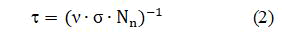
Where σ=10-14 см-2 localized layers of surface charge carriers holding section: ν-pits thermal velocity: ν~107 см/с. Nn=NCu=1 ÷ 20∙1013 cм-3 concentration of copper centers varying in diffusion temperature range. In this case decreases from τ-10-6 to 5∙10-8 seconds.
In the presence of sticky surfaces and recombination centers, their location relative to the Fermi level is shown in Figure 2. Recombination centers (1) and cleavage centers (2) are shown at levels.

Figure 2: Dependence of adhesion and recombination levels on Fermi level in darkness and Fermi quasi-level in light.
When illuminated, the Fermi quasi levels decreases as the electrons fall on the sticky centers as they move upward. However, if the adhesive levels are much higher than the Fermi level, the sample will not fill even when irradiated. Rather (Figure 2b) level 3 is above the Fermi level in the dark and below when it is lit. The presence of 3 levels leads to a significant reduction in the life of the charge carriers, but when they are lit, they do not have sticky surfaces.
If the 2nd levels mentioned in Figure 2b are added Figure 2c, a decrease in τ is not observed. The decrease in τ occurs only when the concentration of electrons captured by the 2 centers is the same.
Thus, based on the analysis of the three mechanisms considered, we conclude that the increase in the life of the charge carriers after hightemperature diffusion relative to the silicon obtained for the test results in the formation of sticky surfaces formed by copper+oxygen complexes. A similar situation is observed in iridium, but the sticky surfaces formed by iridium are not dependent on oxygen.
Figure 3 shows the probability of binding of 1/τ charge recombination to the dose of γ-radiation of the tested and doped samples. This figure shows that the change in the lifetime of the charge carriers depends on the dose of γ-radiation in the samples p- Si<P,B>, p-Si<P,B,Cu> and p-Si<P,B,Ir>, the curves The magnitude of the coefficient of radiation (radiation) Кτ of the change in residence time was determined.

Figure 3: p-Si<P,B>(1,2), p-Si<P,B,Cu> (4) and p-Si<P,B,Ir> (3) τ/τ0 dose dependence of g-radiation in samples, thermal diffusion Тdif=1275°С.
In experiments, Кτ magnitude (Δ1/τ)/ΔF dose dependence was determined in the given areas. The change in the lifetime of the charge carriers in alloy and silicon at a dose of ~ 4 см2 in the initial radiation phase was determined by the following formulas (Figure 4).

Figure 4: Δ1/τ p-Si<P,B> (1,2), p-Si<P,B,Ir > (3,4,5,6) and p-Si<P,B,Cu> (7,8,9,10) were rapidly cooled (2,4,6,8,10) and slowly cooled (1,3,5,7,9). γ-radiation dependence of diffused samples at different
temperatures, 1,2,3,7-1075℃, 4, 8 -1175°С, 5,9, -1275°С and 6,10-1285°С.
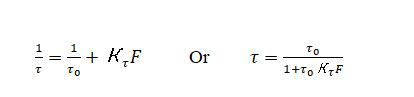
Here τ and τ0 are the pre and post-irradiation lifetimes of the charge carriers, F–γ is the fluorescence of the charge, Кτ is the lifetime of the charge carriers, γ is the coefficient of variation of the radiation, the values of which are given in Table 3.
| Samples | ρ, Ω∙cm |
Тdif.. ℃ |
Cooling speed, grad/min | N, сm-3 | τ0, s |
Кτ, сm2/s |
|
|---|---|---|---|---|---|---|---|
| Ngen. | Nakt. | ||||||
| p-Si<B,Р> | 10 | 1075 | 250 | 5∙1017 | 2∙1013 | 1,2∙10-7 | 9,5∙10-12 |
| p-Si<B,Р,Ir> | 10,1 | 5∙1016 | ≤1012 | 5∙10-5 | 5,4∙10-12 | ||
| p-Si<B,Р,Сu> | 9,8 | 4,6∙10-6 | 7,8∙10-12 | ||||
| p-Si<B,Р > | 10 | 1175 | 250 | 1,4∙10-6 | 9,1∙10-12 | ||
| p-Si<Р, Ir > | 9,1 | 9∙1017 | 1014 | 3,2∙10-7 | 1,2∙10-12 | ||
| p-Si<Р, Сu> | 8 | 8∙1013 | 4,5∙10-6 | 1,9∙10-12 | |||
| p-Si<B,Р,Ir> | 13 | 2∙1014 | 3,2∙10-7 | 6,4∙10-12 | |||
| p-Si<B,Р,Сu> | 12,8 | 1014 | 4,5∙10-6 | 9,8∙10-12 | |||
| p-Si<B,Р> | 11 | 1275 | 250 | 1,2∙1018 | 1,6∙10-6 | 4,5∙10-12 | |
| p-Si<Р,Ir> | 9,8 | 6∙1013 | 5,9∙10-7 | 2,9∙10-13 | |||
| p-Si<Р,Сu> | 9,6 | 1014 | 6,8∙10-6 | 3,3∙10-13 | |||
| p-Si<B,Р,Ir> | 15,8 | 4∙1014 | 3,2∙10-7 | 5,4∙10-13 | |||
| p-Si<B,Р,Сu> | 13,2 | 3∙1014 | 4,5∙10-6 | 8,8∙10-13 | |||
| p-Si<B,Ir> | 25 | 1285 | 250 | 1,8∙1018 | 7∙1014 | 7,3∙10-5 | 1,5∙10-13 |
| p-Si<B,Сu> | 16 | 4∙1014 | 9,2∙10-6 | 2,7∙10-13 | |||
| p-Si<B,Р,Ir> | 3500 | 1,5∙1015 | 3,2∙10-7 | 7,4∙10-13 | |||
| p-Si<B,Р,Сu> | 250 | 8∙1014 | 4,5∙10-6 | 2,8∙10-14 | |||
Table 3: Previous and next parameters of p-type doped and controlled silicon γ-radiation.
It can be seen from Table 3 that as the value of Кτ decreases with increasing copper and iridium concentrations in silicon with doped, the value of Кτ in silicon with doped becomes lower than in the sample under the test. This can be explained as follows: a scheme of quasichemical reactions that occur under the influence of thermal and radiation radiation in doped silicon is proposed (Figure 5).

Figure 5: Defect formation in doped silicon quasi-chemical node and interstitial mixed atoms Хs–, Хi –; МММ-clusters; various mixed atoms of silicon Sii; W–divacancy; MSi-cilicides; Mixtures that form M–CHES; [W+O+Cb]-K-center
Conclusion
It was observed that the concentration of copper and iridium inclusions previously added to silicon doped with neutron was higher than that of ordinary silicon. This was explained by the vacancies created as a result of the radiation.
For the first time, it was found that the decay rate in n-Si<B,Р,Ir> and n-Si<B,Р,Сu> samples was slower than in n-Si<Р,Ir> and n- Si<Р,Сu> samples. This was explained by the magnification of the potential barrier between the high and low Ohm resistance areas.
It was found that the potential barrier of copper-enriched samples of silicon previously doped with neutrons were 5 times larger than that of copper-enriched samples of ordinary silicon.
Thermostability was observed in the temperature range 250-300°C during type II samples, and the increase in lifetime and stability of charge carriers after high temperature diffusion relative to silicon doped with neutron was explained by the formation of adhesive surfaces formed by copper+oxygen complexes.
Thus, based on the obtained results, it will be possible to deepen the knowledge about the occurrence of electro physical phenomena in doped silicon and the production of new thermostable semiconductor devices in agriculture.
References
- Tatokhin EA, Budanov AV, Butusov IY, Vasileva LV, Tutov EA (2008) Voronezh State University Bulletin, series. Phys Math 2:60-70.
- Zaynabidinov SZ, Kurbanov AO (2019) Cluster atomic primes of nickel and ix influence on recombination properties of silicon. Nat sci 2:81-93.
- Yunusov MS, Karimov M, Djalelov MA (2001) Saint Petersburg. J Semicond Phys Technol 35:317-320.
- Ahmadovich MS (2012) Influence of methods on electrophysical and recombinant properties of silicon in thermo and radiation conditions: dissertation. Institute of Nuclear Physics Academy of Sciences of the Republic of Uzbekistan, Tashkent, Uzbekistan, 126.
- Milns A (1977) Impurities with deep levels in semiconductors, Ed. doc. phys.-mat. science M.K. Sheinkman. Mir, Moscow, 502.
- Karimov M, Makhkamov Sh, Tursunov NA, Makhmudov SA, Begmatov KA, et al. (2009) Kinetics of photoconductivity relaxation in n-type silicon compensated by phosphorus atoms. Proceedings of universities. Physics 5:9-12.
- Utamuradova SB, Daliev KS, Fayzullaev KM (2019) The influence of chromium and iron atoms on the processes of defect formation in silicon. Phys Mater Sci Appl Phys 6:90-95.
- Kozhemyako AV, Evseev AP, Balakshin YV, Shemukhin AA (2019) Physics and technology of semiconductors. 6:810.
- Istratov AA, Weber ER (1998) Electrical properties and recombination activity of copper, nickel and cobalt in silicon. Appl Phys A 66:123-136.
- Sukhorukov AV, Ejevskiy AA, Gusev AV, Guseynov DV, Popkov S (2010) Processes of spinal relaxation electron conduction in silicon with different isotopic composition. J Bull Nizhny Novgorod Univ 5:335-338.
- Dzhuplin VN (2000) Defect formation in silicon under nickel films during heat treatment. Tech Sci 5:16-21.
- Zaynabidinov SZ, Daliev XS (1993) Defective formation in silicon. University, Tashkent,190.
- Zainabidinov S (1984) Physical foundations of the formation of deep levels in silicon. Fan Tashkent, 168.
- Lang DV (1974) Deep‐level transient spectroscopy: A new method to characterize traps in semiconductors. J Appl Phys 45:3023.