 Spanish
  Chinese
  Russian
  German
  French
  Japanese
  Portuguese
  Hindi
Hindi Research Article, J Nanomater Mol Nanotechnol Vol: 5 Issue: 6
2D Simulation of Fowler-Nordheim Electron Emission in Scanning Probe Lithography
| Steve Lenk*, Marcus Kaestner, Claudia Lenk, Tihomir Angelov, Yana Krivoshapkina and Ivo W Rangelow | |
| Department of Micro- and Nanoelectronic Systems, Institute of Micro- and Nanoelectronics, Faculty of Electrical Engineering and Information Technology, Technische Universität Ilmenau, Gustav-Kirchhoff-Str. 1, 98693 Ilmenau, Germany | |
| Corresponding author : Steve Lenk
Department of Micro- and Nanoelectronic Systems, Institute of Micro- and Nanoelectronics, Faculty of Electrical Engineering and Information Technology, Technische Universität Ilmenau, Gustav-Kirchhoff-Str. 1, 98693 Ilmenau, Germany Tel: +49 3677 69-1658 Fax: +49 3677 69-3132 E-mail: steve.lenk@tu-ilmenau.de |
|
| Received: June 21, 2016 Accepted: September 13, 2016 Published: September 18, 2016 | |
| Citation: Lenk S, Kaestner M, Lenk C, Angelov T, Krivoshapkina Y, et al. (2016) 2D Simulation of Fowler-Nordheim Electron Emission in Scanning Probe Lithography. J Nanomater Mol Nanotechnol 5:6. doi:10.4172/2324-8777.1000201 |
Abstract
2D Simulation of Fowler-Nordheim Electron Emission in Scanning Probe Lithography
For the manufacturing of quantum computers it will be necessary to routinely fabricate devices with critical dimensions down to the single-digit nanometer range. Since the high-costs and belated development of extreme UV lithography, we are focused on scanning probe lithography (SPL) utilizing Fowler-Nordheim emitted electrons for patterning of molecular resist materials. Our method is similar to the electron beam lithography with special electron emitters, i.e. our nanotips, differing in the much lower energy of the emitted electrons and the possibility to work at ambient conditions. Based on the thermo-mechanically actuated, piezoresistive cantilever technology our group has developed a first prototype of a scanning probe lithography platform able to image, inspect, align and pattern features down to single nanometer regime. Here, we present theoretical investigations of the electron emission and the surface exposure with the emitted electrons. Our simulation model and the used assumptions are described. The resulting electric field and electron density distributions are analyzed to gain deeper insights into relevance of the lithographic exposure parameters.
Keywords: Fowler-Nordheim emission; Simulation; Nanolithography; Scanning probe lithography; Current density distribution; Electric field calculation; Self-actuating piezoresistive cantilever; Active cantilever
Keywords |
|
| Fowler-Nordheim emission; Simulation; Nanolithography; Scanning probe lithography; Current density distribution; Electric field calculation; Self-actuating piezoresistive cantilever; Active cantilever | |
Introduction |
|
| One of the most important tasks to enable novel nanoelectronics, NEMS, photonics and bio nanotechnology based devices is the ability to fabricate features in sub-10 nm regime in a reproducible manner [1,2]. Feature sizes down to 10 nm and below, enable the use of quantum based effects like quantized excitations, single-atom electron spin qubit in silicon, and Coulomb blockade and single-electron tunneling [2]. However, manufacturing methods are currently far away from realising the requirements to generate, overlay and inspect features in the single-nanometer regime [3,4]. | |
| Our group is working on a novel scanning probe lithography method (a scheme is shown in Figure 1), in which self-actuated, selfsensing active cantilever technology [5,6,7] is applied. One of our specially developed cantilevers is depicted in Figure 2. In general, scanning probes are able to confine the tip-sample interaction for imaging, probing and lithography to atomic scales as demonstrated by using scanning tunneling microscopy (STM) [8], as well as atomic force microscopy (AFM) [9] methods. However, the industrial application is strongly limited by extremely low throughput (comparison of lithographic methods concerning patterning speed is provided in [10]), ultra-high vacuum conditions, ultra-low temperatures as well as the lack of pattern transfer capabilities. Within the last two decades numerous tip-based nanofabrication methods have been developed using thermo-mechanical interactions [11], mechanical displacement like nanoshaving / nanografting [12], electric field-induced deposition [13,14], chemical modification by local anodic oxidation [15], local resist exposure using tip-emitted low energy electrons [16,17], to mention only a few. In ref. [18] a more detailed overview about different SPL technologies can be found. | |
| Figure 1: Schematic layout of the closed loop scanning probe lithography platform utilizing a thermally actuated, piezoresistive cantilever (taken from [19]). | |
| Figure 2: SEM image of the active cantilever with integrated thermal bimorph actuation (colored red), piezoresistive readout (colored green). A sub-10 nm read /write tip in right SEM image provides the required resolution capability in both operation modes. The tip is connected with a separated connection line, colored in blue. Scale bars: Overall cantilever SEM image: 50 µm, Zoom-in onto the cantilever tip SEM image: 50 nm (taken from [19]). | |
| Recently, we successfully demonstrated a development-less patterning scheme by using a scanning probe lithography technique based on the electric field emission of electrons exposing the molecular glass resist, Calixarene [1,2,19-25]. The generated high, non-uniform electric field causes a current of low-energy electrons from the tip to the sample surface. This electron exposure triggers the direct patterning process of a calixarene resist film. We are able to switch between cross-linking of the resist (negative tone patterning), which is similar to reported electron beam [26] or extreme ultraviolet (EUV) lithography results [27], and a direct removal reaction (positive tone patterning, development-less). Switching is provided by changing the lithographic exposure conditions [19-25]. In addition, AFM imaging possibilities using the same tool and cantilever allow the inspection of the generated features. In this terms, a closed loop lithography scheme is enabled [21]. Moreover, our group showed sub-5 nm pattern capability of line and dot features [2,10,19,24], mix and match of our SPL and EBL / EUV lithography to enhance the throughput [10] as well as the practical application for pattern transfer by plasma etching [24]. | |
| Based on our experimental expertise we consider the physical mechanisms behind our lithography technique to improve stability and resolution. In this article, we are showing our recent simulation results based on a two-dimensional calculation method, which combines the Fowler-Nordheim emission process and the computation of electron trajectories. Results of the highly localized electric field and the electron density at the tip and the surface are shown. | |
| In this work, a calculation model based on our experimental setup for field-emission scanning probe lithography (FE-SPL) was developed and the results are reported. | |
| The following assumptions are used in our model: | |
| Influence of the resist film on the sample surface and additional contaminations, which might occur at ambient conditions and might affect the electric field and current density distribution, are not considered. | |
| We neglect the electronic energy distribution inside the nanotip and assume that the initial electrons have Ekin=0 eVand are emitted perpendicular to the tip surface. | |
| For a total emission current I=30 pA approximately 150 000 electrons are emitted in a time of t=1 ms, i.e., each electron has around 7 ns before the next electron is emitted. Since the tip-sample distance is in the range of tens of nanometer, the time of flight for an electron with Ekin=10 eV would be below 100 fs. On the other hand the mean free-path in air (ambient conditions) should be well above 100 nm. Therefore, we assume a ballistic transport of electrons between tip and sample. | |
| Since the de Broglie wavelength |
|
| The two-dimensional calculation model is depicted in Figure 3. The tip is characterised by the tip radius 8.5 rtip = nm, the length of the tip (conus) ltip = nm, the opening angle γ =20º and the work function E = −∇φ for the tip material tungsten. The tip-sample distance d is varied from 10 to 100 nm and the bias voltage V=10…100 V, which is applied at the sample. | |
| Figure 3: Nanotip model used in the simulation. | |
| The computation of the electric field E = −∇φ is based on a two dimensional solution of Laplace’s equation ∇φ = 0 for the electrostatic potential φ [29,30]. This is done by using the PDE toolbox of MATLAB®. The geometry shown in Figure 3 is used for the finite-element method calculation. The boundary conditions are adapted to the model and the applied bias voltage. | |
| The Fowler-Nordheim emission current density [31,32,33] is based on following equation | |
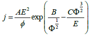 (1) (1) |
|
| Here, A, B and C are constants taken from [33]. | |
| The trajectories of the electrons are computed by the help of a Velocity-Verlet algorithm [34] by using the calculated 2D electric field strength. | |
| In Figure 4 the electric field strength (in V/nm) is shown colorcoded for a tip-sample separation of 100 nm and a bias voltage of V=30 V. The enormous field strengths, which appear at the tip apex, are in a range of a few V/nm due to the lightning rod effect [35-37]. | |
| Figure 4: Calculated electric field strength (in V/nm) for a tip-sample distance d=100 nm and an applied bias voltage of 30 V. | |
| Additionally, it can be seen that the field strength decreases rapidly with increasing distance to the tip. This decrease is approximately linear far away from the tip. In Figure 5 we show the electric field strength distributions (as color-code) for applied bias voltages of 30 V and 50 V. The tip sample distance was held constantly at d=10 nm. An identical scale bar for the electric field strength was used for both voltage values. An increase of the electric field by increasing bias voltage is obvious. | |
| Figure 5: Calculated electric field strength for a tip-sample distance d=10 nm and an applied bias voltage of (a) 30 V and (b) 50 V. The scale bar of the color-coded electric field strength is identical in for (a) and (b). | |
| By comparing Figure 4 and 5(a), in which the voltage is kept constantly at 30V and the separation decreased, it is worth to note that the electric field strength at the sample surface is highly influenced by the close proximity of the tip. | |
| The electron trajectories the current density distribution j is additionally shown in Figure 6. As expected a major part of the electrons is emitted closely to the tip apex, where at the smallest distance the strongest electric field found to be present. In Figure 6(b) it is also clearly visible that the electron distribution exceeds the diameter of the nanotip even though, in principle, no electrons were emitted at the side of the tip. This can be explained by the direction of the emitted electrons. All electrons are emitted perpendicular to the tip surface as it is depicted in Figure 6(a) and due to our assumptions with zero kinetic energy. Since the electrons are accelerated in the electric field and the electric field lines are also perpendicular to the tip surface, an initial broadening of the electron distribution is observed. One main difference between the field lines and the trajectories is that the field lines enter the sample perpendicular as well, but the electron trajectories do not. This behavior has its origin in the inertial mass of the electrons. | |
| Figure 6: The color-coded electric field strength is shown together with the electron emission probability at the nanotip (a). The electric field with some possible electron trajectories (black) and the electron density distribution (red) is shown in (b). The tip-sample separation is 35 nm and the applied voltage 50 nm. | |
| By integration over the current density distribution we obtained the total current ranged in the pA scale. In Figure 7 we plotted the maximal electric field strength (black) and the logarithm of the total current (red) over the tip-sample separation. The behavior of the electric field resembles the dependency known from capacitors. The total current shows much stronger non-linearity than the electric field. This behavior is caused by the exponential part of the current density distribution i.e. j is proportional to E2 exp(-1/E) (see eq. 1). It explains the restriction to a small parameter range for high-resolution FE-SPL, since a small change of the tip-space distance is strongly affecting the current density and, thus, the resolution. The dependency of the current density on the tip-sample separation is approximated by j is proportional to exp(-d) with a tip-sample distance d ≈10...100nm . | |
| Figure 7: Electric field strength (black) and total current (red) versus the tip-sample distance. The applied bias voltage is 50 V. Figure | |
| The resolution capabilities are shown in Figure 8(a). The “effective” electron beam diameter is plotted versus the tip-sample distance. Different line colors specify different bias voltages. The threshold value for direct removal is defined as the current density distribution, which matches 100 electrons on an area of 1 nm2 for a tip velocity of 5 μm/s. This velocity is normally used in our FE-SPL tool. The number of electrons is an estimate for the amount of electrons needed for direct removal of the Calixarene resist. The “effective” electron diameter is defined as diameter for which the current density distribution exceeds this threshold value. Two regimes can be distinguished in Figure 8(a): on one hand the diameter increases with increasing distance and on the other hand it decreases. The first regime (diameter increase) occurs if the maximal current density distribution is much higher than the threshold value. The distance increase yields a broader current density distribution, i.e. a larger beam diameter. The threshold value plays no important role. The second regime (diameter decrease) appears if the maximal current density distribution is close to the threshold value. If the distance is increased the maximum current density decreases exponentially (see eq. 1) and so does the beam diameter. For maximal current densities smaller than the threshold value no reasonable diameter is definable. The minimal shown diameter is below 10 nm. | |
| Figure 8: (a) Effective electron beam diameter vs. tip-sample distance for different bias voltages (line colours). (b) Fowler-Nordheim plot for different tip-sample separations (line colours and markers). The missing data in (a) and (b) arise from too low current density values (close to zero). | |
| These results are in contradiction with the results from Mayer et al. [33] in which they found only the increase of the beam diameter. This is related to the different definition of the beam diameter; Mayer et al. define the beam diameter by 60% of the maximum total current. However from our experiments we know that a threshold value for the resist removal and also for resist crosslinking is a more realistic scenario. | |
| Since the work function depends on the internal band structure of the material, an often used approach is the estimation of the work function on the basis of Fowler-Nordheim plots [38]. In Figure 8(b) the Fowler-Nordheim plots are shown for different tip-sample distances. It is observable, that even without changing the work function, the slope and the offset varies. Therefore, the extraction of the work function from Fowler-Nordheim plots is not trivial and the tip-sample separation needs to be well-known. We do not show the variations, which occur for different tip radii and opening angles, but the estimation of the work function of the tip material requires the precise knowledge of these parameters. This will be part of an upcoming publication. | |
Summary and Outlook |
|
| In this publication we presented our first theoretical study of the current density distribution, which is our first theoretical effort towards understanding the patterning process using field emission scanning probe lithography. The 2D computational method yields important physical properties related to the field emission and the patterning resolution. The pattern properties are based only on the electron emission and trajectories. We clearly showed the lightning rod effect and the enormous field strengths occurring at the nanotip. The electric field strength exhibits a non-linear dependency on the tip-sample distance. Here, not only the electron emission is triggered by these high electric fields but also their trajectories are strongly affected. It was shown that the electron trajectories differ from the electric field lines due to their inertial mass. The computed total current clearly shows a stronger non-linear dependency on the tip-sample distance compared to the electric field strength. This causes difficulties in finding the optimal parameters for the highest resolution patterning and it clearly proves that the current density depends exponentially on the electric field. The resolution capabilities were studied by assuming a current density threshold value for the lithographic process. The minimal shown effective beam diameter is below 10 nm. Additionally, the Fowler-Nordheim plots identified the difficulty to extract the work function of the nanotip based on the limited knowledge of the geometrical parameters of the tip. | |
| In summary, we are able to forecast some patterning properties using our 2D model. However, the model lacks in several aspects. The 3D natures of the tip as well as the intrinsic properties of the electrons in the tip are not considered. Additionally, the resist influences the electron distribution on the sample as well. This should also be taken into account for a complete lithography simulation. These influences will be studied in future work. Moreover, we would like to investigate the limits of lithographic resolution by taking the interactions between1 electrons and resist materials into account. Further on, the influence of a volcano-type gate will be simulated. [39]. | |
Acknowledgment |
|
| The research leading to these results has received funding from the European Union's Seventh Framework Programme FP7/2007-2013 under grant agreement no 318804 (“Single Nanometer Manufacturing for beyond CMOS devices” -acronym SNM). | |
References |
|
|
|

