Research Article, J Nanomater Mol Nanotechnol Vol: 12 Issue: 1
Nano Moth-eye Structures Fabricated Using Ultra-thin Photoresist and Combined Dry and Wet Etches
Rachit Sood1*, Chaoran Tu1, Douglas Bamford2, Joel Henseley2, David Woolf2, Curtis Menyuk1, NB Singh1 and Fow-Sen Choa1
1Department of Computer Science and Electrical Engineering, University of Maryland, Baltimore County, USA
2Physical Sciences Inc, Massachusetts, USA
*Corresponding Author: Rachit Sood Department of Computer Science and Electrical Engineering, University of Maryland, Baltimore County, 1000 Hilltop circle, Baltimore, MD, 21227, USA, Tel: +1 3015475523 E-mail: Rachi1@umbc.edu
Received date: 25 January, 2023, Manuscript No. JNMN-23-81183;
Editor assigned date: 27 January, 2023, Pre QC No. JNMN-23-81183 (PQ);
Reviewed date: 10 F ebruary, 2023, QC No. JNMN-23-81183;
Revised date: 17 F ebruary, 2023, Manuscript No. JNMN-23-81183 (R);
Published date: 24 February, 2023, DOI: 10.4172/2324-8777.1000343
Citation: Sood R, Tu C, Bamford D, Henseley J, Woolf D, et al (2023) Nano Moth-eye Structures Fabricate: Using Ultra-thin Photoresist and Combined Dry and Wet Etches. J Nanomater Mol Nanotechnol 12:1.
Abstract
Anti-Reflective (AR) coatings are used to suppress reflection and enhance optical transmission, but many coatings cannot withstand harsh environmental conditions. In this work, we report the fabrication of nanostructures on Gallium Arsenide (GaAs) via contact photolithography for anti-reflection applications in the mid-infrared (mid-IR) range. An E- beam mask was used to lithographically transfer nano-structure patterns to a SiO2 etching mask and then further transfer the structure to gallium arsenide wafers. With a thin layer Photo Resist (PR) along with a combination of Reactive Ion Etching (RIE) and wet Buffered Oxide Etching (BOE), we were able to transfer the nanostructure patterns from the thin PR to the thick SiO2 etching mask and then onto a wafer. The fabricated structures are squares and hexagons of feature size 900 nm, 1000 nm, 1100 nm, and the gap between two neighboring shapes is 400 nm. By varying the pitch of the structures, we observe improvement in the transmission over the mid-IR range (500-2000 cm-1 wavenumber). Experimental results of coated and uncoated GaAs are obtained using the Fourier Transform Infrared Spectroscopy (FTIR) while theoretical results of coated GaAs are shown using the Rigorous Coupled Wave Analysis (RCWA). This work provides a better success rate and a more readily available mass production technique to fabricate the sub-wavelength nanostructures. The theoretical results obtained using RCWA agree well with experimental results to show the overall 69% transmission with a one-side coated gallium arsenide wafer.
Keywords: Anti-reflection; Moth eye structures; Mid-IR; fabrication; Photolithography; Wet etching; Newton rings
Introduction
Reflection takes place when light travels from one medium to another due to the refractive index difference between the two media. To reduce reflection and improve transmission, single-layer or multilayer non-absorbing materials are typically coated at the media interface for Anti-Reflection (AR). However, at longer operating wavelengths, these coatings need to be thick, and they can easily crack, which makes this approach unattractive for mid to long infrared wavelengths. Sub-wavelength structures are an alternative way to produce the anti-reflection. In this approach, arrays of periodic structures are arranged whose periods are less than the light wavelength [1-3]. Moth eye structures are bio-mimetic structures whose surfaces are covered with hexagonal nanostructure patterns of bump shapes whose size is smaller than the wavelength of visible light.
The effective refractive index of the meta-material gradually changes from the air refractive index through the continuously changing nanostructure refractive index and then to the substrate refractive index, which helps to suppress reflections. In recent years, a variety of moth-eye structure morphologies have been investigated, including cylindrical, conical, pyramidal, and parabolic [4-6]. Choi et al. fabricated and optimized cone-shaped moth-eye structures to increase the transmittance [7]. Jiang et al. developed a hexagonal shape self-cleaning moth-eye structures on a variety of substrates such as silicon, glass, and GaAs [8]. Chuang et al. reported a one-step colloidal lithography process to fabricate the pyramid shape moth-eye structure [9]. Zhang et al. designed and fabricated the parabola-like moth-eye structures using the UV-NIL technique [5].
A nano dome pattern on a glass substrate was created by Lim et al. using a nanoimprinting process for photovoltaic applications [10]. Moth eye structures have many advantages. First, these structures have low reflection and high transmission at its oblique angle of incidence [11,12]. Second, the performance can be improved over a wide range of wavelengths by optimizing the shapes and parameters of nanostructures [13-15]. Third, since these structures are fabricated directly on the substrate without using foreign material, they can increase the structure’s durability and tolerance in extreme conditions [16-18]. On the other hand, fabricating moth-eye structure can be quite challenging especially at short wavelengths since the feature size is over the nanometer scale. Many lithography techniques are used to fabricate nanostructures such as Nano imprint lithography, Laser Interference Lithography (LIL), e-beam lithography and dip-pen nanolithography [19-24]. However, because of high cost and low throughput, these techniques are unattractive for large-scale production.
In this work, we used contact photolithography, which is a relatively inexpensive and easy technique, to fabricate square and hexagon nanostructures on Gallium Arsenide (GaAs) substrates. Although the mask itself is made using e-beam lithography, a variety of structures with different spatial pitches over a large area can be printed in a single exposure, thereby increasing the throughput. Not many papers in the past have been being published using this technique to obtain the nanostructures on GaAs. Choi et al. fabricated the moth-eye structures using photolithography to improve the transmission of silicon wafers [14]. Most of the research has been on silicon material, while there is very little literature involving the fabrication of GaAs based moth-eye structures [25-32].
Although having a higher refractive index than silicon and glass, GaAs is used in our work as it has many applications in surfaceemitting lasers, photo detectors, and optoelectronic devices like solar cells because of its high conversion efficiency under low light conditions and high thermal conductivity [33-36]. However, because of the higher refractive index of GaAs, more than 30%-35% of the light is being reflected back from the surface, which makes it inefficient in many applications. To improve performance and suppress unwanted reflection losses, we have fabricated the moth-eye nanostructures of various sizes on GaAs substrate. The nanostructures are fabricated using a simple, cost-effective, and robust fabrication method. To successfully accomplish nano-pattern transfers from the Ebeam mask to a 300 nm thick SiO2 etching mask layer, a very thin photoresist of about 50 nm is used for the UV exposure and development which is then followed by dry and wet etches of the SiO2 layer. The patterns are then faithfully transferred to the GaAs substrate using combined Reactive Ion Etching (RIE) and wet etching with procedures that are described in the experimental section [37-43].
Using a very thin photoresist is a necessity not just being more advantageous to faithfully transfer the patterns onto the photoresist and then onto the GaAs wafer. Since the pattern dimension is very close to the diffraction limit i.e. the exposed UV wavelength is compatible with the size of the nanostructure, using a thick photoresist does have serious problems and cannot faithfully transfer the patterns. We have experimentally demonstrated the above fact with 2 gallium arsenide wafers, one has a thicker photoresist layer (over 500 nm thick) and the other has a thin photoresist layer (<50 nm). After exposures, the thin PR wafer has no problem developing clear nanostructure patterns. For the thick PR wafer, the full exposed window can be developed but it cannot obtain nanostructure patterns, as a result of the diffraction interference. Figure 1 shows the 2 GaAs samples: one with PR of less than 50 nm and another with PR of about 500 nm. To our knowledge, no previous work has reported less than 150 nm thick PR for photolithography fabrication that is close to diffraction-limited nanostructure.
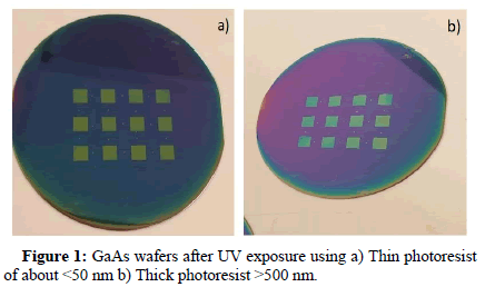
Figure 1: GaAs wafers after UV exposure using a) Thin photoresist of about <50 nm b) Thick photoresist >500 nm.
The paper is organized as follows: In the experimental section, we show the design of the nanostructures and report the detailed fabrication of the nanostructures on GaAs substrates. In sec. 3, we show the SEM images of the fabricated structures. Theoretical results are obtained using a Rigorous Coupled-Wave Analysis (RCWA) computational method and are shown in the results section along with the experimental results [44,45]. The RCWA method analyzes the reflectance and transmittance of an electromagnetic plane wave incident obliquely on a grating structure composed of materials with different indices. Finally, sec. 4 contains the conclusion.
Materials and Methods
Experimental setup
Design: Nanostructures are designed using an AutoCAD design tool. Our design consists of square and hexagon shapes with spatial pitch 900 nm, 1000 nm, and 1100 nm. The gap is 400 nm. In Figure 2, we show the array of periodic structures fabricated on a glass photomask. The shapes are arranged in 5 mm × 5 mm square boxes.
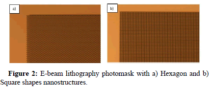
Figure 2: E-beam lithography photomask with a) Hexagon and b) Square shapes nanostructures.
Fabrication of nanostructures
A 3-inch p-type Gallium Arsenide (GaAs) wafer was first cleaned by rinsing the wafer in the acetone and methanol for 5 min followed by rinsing it in Deionized (DI) water, which removed the oils and organic residue from the surface of the wafer. We then deposited a 300 nm thick layer of silicon dioxide on the wafer using Plasma-Enhanced Chemical Vapor Deposition (PECVD) [46]. The sources are 10% silane and nitrous oxide gases. The temperature and Deposition rate of PECVD is about 300°C and 80 nm per minute. We processed the wafer for 3.5 minutes. A silicon dioxide layer on the surface ensures that the patterns can be etched deep enough onto GaAs during the dry/wet etching steps. We spun the wafer for 1 minute in Hexamethyldisilazane (HMDS) at 3000 Revolutions per Minute (RPM) to provide a hydrophobic surface with good adhesion and good wetting. HMDS is a solvent-like liquid, and it is used to clean the surface moisture and help the photoresist stick on the oxide surface. It will not leave a measurable thickness.
Then, we spin-coated the diluted Photo Resist (PR) S1805 on the wafer. We adjusted the dilution ratio and rotation speed to obtain the 50 nm thick PR layer. The spinning speed of 4500 rpm and diluting ratio of 4:1 of Shipley positive thinner propylene glycol monomethyl ether acetate to PR ratio ensures that desired thickness of PR is obtained on the surface of wafer. The e-beam mask with patterned chrome layer was held on top of the photoresist and we exposed the structure to UV light for 5 seconds. The light only exposed the area that is not covered by chrome. The exposed photoresist was developed in 4:1 DI water: AZ400K developer at room temperature.
With a short developing time of ~5 seconds, structures with squares and hexagons with the desired pitch and gap were obtained using conventional photolithography. A non-uniform gap distance distribution between the photomask and the wafer surfaces may create interference patterns which we referred to as newton rings leading to the formation of bright and dark fringes on the photoresist exposure. Due to the weakening of UV light caused by the destructive interference, some parts of the PR will not be fully developed. The problem can be mitigated using a thin layer of photoresist to ensure that patterns are fully developed even with weaker UV intensity. Figure 3 shows square and hexagon-packed structures with labeled feature size and gap between two neighboring shapes.
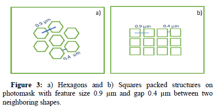
Figure 3: a) Hexagons and b) Squares packed structures on photomask with feature size 0.9 μm and gap 0.4 μm between two neighboring shapes.
The developed photoresist patterns were then used as a mask for combined dry and wet etches to transfer the patterns to the silicon dioxide layer. This step was carried in SF6 gas, maintained at 250 mTorr pressure and 30 W RF power. The wet etching in Buffered Oxide Etcher (BOE) lasted for 75 seconds. BOE is a mixture of ammonium fluoride (NH4F) and Hydrofluoric Acid (HF). In our processing, we used 7:1 BOE supplied by JT Baker. After that, we etched the GaAs substrate using the SiO2 layer as the mask. We used an Induced Coupled Plasma (ICP) etcher with SiCl4/Ar mixture gas at a pressure of 3 mTorr to obtain moth-eye shapes with a height of 2000 nm. The etching time was about 10-12 minutes. Finally, we stripped out the SiO2 layer by rinsing the sample in diluted Hydro Fluoric acid (HF) solution. In Figure 4 we show the entire fabrication procedure.
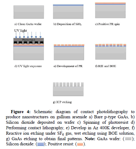
Figure 4: Schematic diagram of contact photolithography to produce nanostructures on gallium arsenide a) Bare p-type GaAs, b) Silicon dioxide deposited on wafer c) Spinning of photoresist d) Performing contact lithography, e) Develop in Az 400K developer, f) Reactive ion etching under SF6 gas, wet etching using BOE solution, g) GaAs etching to obtain final patterns. Note: GaAs wafer: ( ); Silicon dioxide: (
 ); Positive resist: (
 ).
).
Results
To examine the morphology of structures, we used Scanning Electron Microscopy (SEM) to observe the wafer. Figures 5 and 6 show the SEM results for the squares and hexagons fabricated on gallium arsenide. We measured the spatial pitch and gap of the structures using a SEM-calibrated scale. The height of the shapes is around 2000 nm. The edges of the shapes were rounded in all cases due to near-field Fresnel diffraction as shown in SEM images. It was also observed that the fabricated nanostructures have different shapes such as cylinders, pillars, and hexagons. This variation occurs when the distance between photoresist and photomask is not minimized, the interference caused by diffracted light from nearby cells will create undesired effects on pattern transfer. During the photoresist development and SiO2 etching, residue photoresist can cause slower SiO2 etching, which in turn leads to incomplete etching of GaAs. To obtain good and faithful pattern transfer, a tighter force control of the contact between the photomask and photoresist is necessary.
Figure 5a shows square shape patterns with a pattern pitch of 1100 nm. Figures 5b and 5c show the 1000 nm and 900 nm pitch square shape patterns observed at oblique angles. All the square shape patterns after fabrication appear as cylinders.
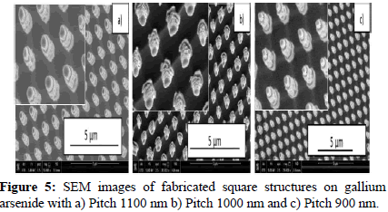
Figure 5: SEM images of fabricated square structures on gallium arsenide with a) Pitch 1100 nm b) Pitch 1000 nm and c) Pitch 900 nm.
Figures 6a and 6b show the hexagonal shapes with a feature size of 1100 nm and 1000 nm. The structures of Figure 6a appear like cylinders when seen at oblique angles while the structures of Figure 6b are hexagons. Figure 6c shows that there are small holes in between the big holes for the structure with hexagonal shapes and a pitch of 900 nm.
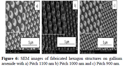
Figure 6: SEM images of fabricated hexagon structures on gallium arsenide with a) Pitch 1100 nm b) Pitch 1000 nm and c) Pitch 900 nm.
It is observed that the array of squares and hexagons of desired pitch and gap are successfully obtained using this simple technique of lithography. To measure the transmission distribution of the structures, we used Fourier Transform Infrared Spectroscopy (FTIR) meter. We also launch a numerical simulation using Rigorous Coupled-Wave Analysis (RCWA) to compare the results. The simulation model is shown in Figure 7 the RCWA is a semi-analytical Fourier space method that can be used to find exact solutions for electromagnetic waves that diffract through intricate grating structures [47]. In our studies, we placed 36 pillars on the gallium arsenide substrate to get an accurate simulation result. For each unit pillar with the square profile or the hexagon profile, we build a matrix where the analytical Fourier series are stored. The unit computational region is the product of pitch by pitch. We begin our analysis by calculating the Fourier series for a given permittivity distribution. The permittivity is assumed to be constant along the z-direction. The Fourier decomposition of this function can either be done analytically or by using the Fast Fourier Transform (FFT) algorithm. The wavenumbers for the electric and magnetic fields are expanded as pseudo-periodic functions using the Floquet-Bloch theorem, which describes a wave function traveling across a periodic lattice [48-50]. The height of the moth-eye structure and gap between two neighboring moth eyes is fixed to 2 μm and 0.4 μm, respectively. We varied the array shape and pitch in order to find the optimal parameters for broadband infrared transmission.
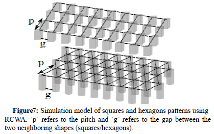
Figure 7: Simulation model of squares and hexagons patterns using RCWA. ‘p’ refers to the pitch and ‘g’ refers to the gap between the two neighboring shapes (squares/hexagons).
The period is varied from 0.9 μm to 1.1 μm. It is observed that the average transmission is higher for smaller pitch structures because the modulation effect is strong for smaller pitch structures. The large period structures exhibit weak modulations and therefore transmission is less [51]. To investigate how the shapes are affecting the transmission, we compared the structures of squares and hexagons of pitch 1.0 μm.
Figure 8 shows the transmission spectra of squares and hexagons of pitch 1.0 μm and gap 0.4 μm. The average transmission of hexagons shapes structures is more than the square shape structures for broadband mid IR wavelength. This is because hexagonal packing scheme provide the better impedance matching than the square packing scheme [52-54]. The effect of shape on transmission can further be explained using the concept of effective medium theory which states that any abrupt change in effective refractive index reduces the transmission [55-59]. Since the cylindrical shape profile Figure 5b shows the abrupt change at the top of the pillar nanostructure and then maintained a constant value from the top to the bottom, therefore, a large discontinuity in refractive index exists which contributes to the reflection [51,60]. However, for hexagonal shape profile (Figure 6b), the effective refractive index gradually changes from top of the structure array to the bottom which results in higher transmission than that of cylindrical shape profiles.
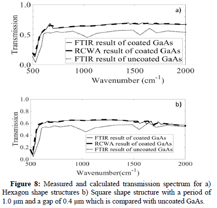
Figure 8: Measured and calculated transmission spectrum for a) Hexagon shape structures b) Square shape structure with a period of 1.0 μm and a gap of 0.4 μm which is compared with uncoated GaAs.
The average transmission of 23% more is achieved for coated GaAs compared to uncoated GaAs. As shown in Figure 8a, the peak transmission is observed in the region 700-2000 cm-1 where transmission increases from 58% to 69% (about 70% between the regions 1400-1700 cm-1). In theory, the maximum transmission of one side AR coated GaAs is about 71% [17]. In the next phase, we will employ the same method to pattern the structures on both sides of GaAs and compare the results. The proposed lithography technique can apply for much broader applications. To replicate the structures on other types of wafers, there is no major issue in patterning. However, etching of structures and etching duration will depend upon the materials (silicon dioxide in our case) used as etching masks.
Surface relief microstructures by Douglas et al. were fabricated using interference lithography [16]. The Transmission was measured for the mid-IR range and a maximum of 70% transmission was achieved [17]. About 62% transmission was observed for 5 μm (2000 cm-1 wavenumber) wavelength compared to nearly the same transmission when the nanostructures are fabricated using the contact lithography. The reflectivity is shown in many previous studies for nanostructures fabricated on different substrates (Si, glass, ZnGeP, As2Se3) for short and long wavelengths [5,16,61]. The major advantage of using contact lithography is its low cost and easy-to-use technique compared to alternative approaches.
The transmission and reflectivity results are shown for single, multilayer, and moth-eye nanostructures [18]. Single layer AR coating shows a maximum of 97% transmission compared to 98% transmission observed for moth-eye structure. The 99% transmission for multilayer AR coatings is optimal, however, it is very sensitive to the angle of incidence, and AR performance does not exhibit for broad spectral range [18].
Discussion
In extreme conditions like large temperature change, AR coatings couldn’t withstand because the moisture and different thermal expansion rates can cause the surface layer to partially detach or peel off from the host material. However, moth eye structures built on the same surface without involving other material can overcome this issue. The stability and durability of the structures in previous studies were examined through immersion tests and observed that the optical properties of nanostructure coating are unaffected in strong acid or alkali environments making it suitable to withstand the harsh environmental conditions. These coatings also exhibit a self-cleaning property in varied environments [17,18,61-63]. AR performance for single layer and moth-eye structure are compared in different environmental conditions: extreme heat, saturated humid heat, and humid heat [17]. In all three tests, moth-eye structure shows a better performance than the single layer AR coatings. Although multi-layer AR coatings have slightly better transmission gain, the other downsides of high sensitivity and low stability under extreme heat make the moth-eye structures a better solution in terms of angular tolerance and AR performance.
Anti-Reflection (AR) in the Infrared (IR) region has been used for a variety of applications such as micro lens integrated detectors, laser facets, solar cells, and other optoelectronic devices [64,65]. For Gallium Arsenide (GaAs), it has excellent characteristics for parametric frequency conversion and is potentially one of the most attractive mid-IR nonlinear optical materials [66]. Orientation- Patterned Gallium Arsenide (OP-GaAs) crystals are most often antireflection coated on their input and output facets which is used in nonlinear frequency conversion in the mid-IR region [67-69].
Conclusion
We fabricated moth-eye structures on gallium arsenide substrates using a simple, cost-effective and readily available lithography technique. We used a thin photoresist layer with a thickness of 50 nm to minimize the newton ring interference effect and to faithfully transfer the E-beam mask patterns to GaAs wafers. We developed structures with square and hexagon shapes with pitches of 900 nm, 1000 nm, and 1100 nm and a height of 2000 nm. Experimental measurements along with theoretical results show that the transmission through the GaAs increases to 69% over the wavelength range of 5 μm to 10 μm, which is close to the maximum transmission of GaAs. Based on our best knowledge, without using holography technique, no previous work has experimentally achieved near 69% transmission with fabricated moth-eye structures. The thorough experimental and theoretical results show that the cost-effective mass production lithography technique is a viable approach to fabricate nano-arrays. The improved transmission will be helpful in optoelectronic applications.
Acknowledgement
This material is based upon work supported by United States air force under contract number FA8650-19-C-1946. Any opinions, findings and conclusions or recommendations expressed in this material is those of the authors) and do not necessarily reflect the views of United States air force.
References
- Bernhard CG, Miller WH (1962) A corneal nipple pattern in insect compound eyes. Acta Physiol Scand 56: 385-386.
[Crossref] [Google Scholar] [Indexed]
- Wilson SJ, Hutley MC (1982) The optical properties of 'moth eye' antireflection surfaces. Optica Acta 29: 993-1009.
- Clapham PB, Hutley MC (1973) Reduction of lens reflexion by the 'Moth Eye' principle. Nature 244: 281-282.
- Shi G, Chen J, Wang L, Wang D, Yang J, et al. (2016) Titanium oxide/silicon moth-eye structures with antireflection, p-n heterojunctions and superhydrophilicity. Langmuir 32: 41.
[Crossref] [Google Scholar] [Indexed]
- Zhang C, Yi P, Peng L, Ni J (2017) Optimization and continuous fabrication of moth-eye nanostructure array on flexible polyethylene terephthalate substrate towards broadband antireflection. Appl Opt 56: 2901-2907.
[Crossref] [Google Scholar] [Indexed]
- Leem JW, Song YM, Yu JS (2011) Six-fold hexagonal symmetric nanostructures with various periodic shapes on GaAs substrates for efficient antireflection and hydrophobic properties. Nanotechnology 22: 485304.
[Crossref] [Google Scholar] [Indexed]
- Choi JS, An JH, Lee JK, Lee JY, et al. (2020) Optimization of shapes and sizes of moth- eye-inspired structures for the enhancement of their antireflective properties. Polymers (Basel) 12: 296.
[Crossref] [Google Scholar] [Indexed]
- Jiang B, Min WL, Jiang P (2008) Bioinspired self-cleaning antireflection coatings. Advanced Materials 20: 3914-3918.
- Chuang SY, Chen HL, Shieh J, Lin CH, Cheng CC, et al. (2010) Nanoscale of biomimetic moth eye structures exhibiting inverse polarization phenomena at the brewster angle. Nanoscale 2: 799-805.
[Crossref] [Google Scholar] [Indexed]
- Lim J, Sun-Mi L, Ho-Young J, Seok-Min K (2015) Fabrication of an antireflective nanodome array with high packing density for photovoltaic applications. J Nanomat 2015: 6
- Sai H, Fujii H, Arafune K, Ohshita Y, Kanamori Y, et al. (2007) Wide-Angle antireflection effect of subwavelength structures for solar cells. Jpn J Appl Phy
- Zhaoning Y, He G, Wei W, Haixiong G, Stephen YC (2003) Fabrication of large area subwavelength antireflection structures on Si using trilayer resist nanoimprint lithography and liftoff. 21: 2874-2877
- Weiblen RJ, Menyuk CR, Busse LE, Shaw LB, Sanghera JS, et al. (2016) Optimized moth-eye anti-reflective structures for As2S3 chalcogenide optical fibers. Opt Express 24: 10172-10187.
[Crossref] [Google Scholar] [Indexed]
- Pengcheng Zhang, Qiuling Wen, Xipeng Xu, (2020) Parameters optimization of nanopatterned sapphire substrates for enhancing light extraction efficiency of GaN-based LEDs. Opt Commun 464: 125548.
- Douglas SH, Bruce DM, Juanita RR (2007) Update on the development of high performance anti-reflecting surface relief micro-structures. Proc SPIE Window and Dome Technologies and Materials X.
- Ren T, He J (2017) Substrate-Versatile approach to robust antireflective and superhydrophobic coatings with excellent self-cleaning property in varied environments. ACS Appl Mater Interfaces 9: 34367-34376.
[Crossref] [Google Scholar] [Indexed]
- Ducros C, Brodu A, Lorin G, Emieux F, Pereira A (2019) Optical performances of antireflective moth-eye structures. Comparison with standard vacuum antireflection coatings for application to outdoor lighting LEDs. Surf Coat Technol 379: 125044,
- Zhang C, Peng L, Lai X, Ni J (2015) Fabrication of moth-eye nanostructure arrays using roll-to-roll uv-nanoimprint lithography with an anodic aluminum oxide mold. IEEE Transactions on Nanotechnology 14: 1127-1137.
- Xu J, Wang ZB, Zhang Z, Wang DP, Weng ZK (2014) Fabrication of moth-eye structures on silicon by direct six-beam laser interference lithography. J App Phys 115: 203101–203101.
- Liu K, Avouris P, Bucchignano J, Martel R, Sun S, et al. (2002) Simple fabrication scheme for sub-10 nm electrode gaps using electron beam lithography. Appl Phys Lett 80: 865–867.
- Taniguchi J, Yamauchi E, Nemoto Y (2008) Fabrication of antireflection structures on glassy carbon surfaces using electron beam lithography and oxygen dry etching. J Phy Conf Ser 106: 012011
- Hyungil J, Dalal CK, Steven K, Raman S, Patrick CC (2004) Surfactant activated dip-pen nanolithography. Nano Lett 4: 2171-2177.
- Chen L, Wei X, Zhou X, Xie Z, Li K, et al. (2017) Large-area patterning of metal nanostructures by dip-pen nanodisplacement lithography for optical applications. Small 13: 1702003
[Crossref] [Google Scholar] [Indexed]
- Sun C, Min W, Linn N, Jiang P, Jiang B (2007) Templated fabrication of large area subwavelength antireflection gratings on silicon. Appl Phys Lett 91: 231105.
- Lin YR, Wang HP, Lin CA, He JH (2009) Surface profile-controlled close-packed Si nanorod arrays for self-cleaning antireflection coatings. J Appl Phys 106: 114310
[Crossref] [Google Scholar] [Indexed]
- Hadobas K, Kirsch S, Carl A, Acet M, Wassermann EF (2000) Reflection properties of nanostructure-arrayed silicon surfaces. Nanotechnology 11: 161-164
- Song YM, Yu JS, Lee YT, (2010) Antireflective submicrometer gratings on thin-film silicon solar cells for light-absorption enhancement. Opt Lett 35: 276-278
[Crossref] [Google Scholar] [Indexed]
- Lalanne P, Morris GM (1997) Antireflection behavior of silicon subwavelength periodic structures for visible light. Nanotechnology 8: 53-56.
- Sai H, Fujii H, Arafune K, Ohshita Y, Yamaguchi M, et al. (2006) Antireflective subwavelength structures on crystalline Si fabricated using directly formed anodic porous alumina masks. Appl Phys Lett 88: 201116.
- Sun CH, Ho BJ, Jiang B, Jiang P (2008) Biomimetic subwavelength antireflective gratings on GaAs. Opt Lett 33: 2224-2226.
[Crossref] [Google Scholar] [Indexed]
- Song YM, Bae SY, Yu JS, Lee YT (2009) Closely packed and aspect-ratio-controlled antireflection subwavelength gratings on GaAs using a lenslike shape transfer. Opt Lett 34: 1702-1704
[Crossref] [Google Scholar] [Indexed]
- O'Daniel JK, Smolski OV, Johnson EG (2006) High efficiency dual-wavelength surface-emitting laser incorporating integrated dual-grating reflector. IEEE Photonics Technol Lett 18: 445-447.
- Wu M, Huang Y, Ho C (2007) High-Speed InGaP/GaAs p-i-n photodiodes with wide spectral range. IEEE Electron Device Lett 28: 797-799.
- Li X, Li P, Ji L, Stender C, Tatavarti SR, et al. (2015) Integration of subwavelength optical nanostructures for improved antireflection performance of mechanically flexible GaAs solar cells fabricated by epitaxial lift-off. Sol Energy Mater Sol Cells 143: 567-572.
- Moon S, Kim K, Kim Y, Heo J, Lee J (2016) Highly efficient single-junction GaAs thin-film solar cell on flexible substrate. Sci Rep 6: 30107.
[Crossref] [Google Scholar] [Indexed]
- Huff M (2021) Recent advances in reactive ion etching and applications of high-aspect-ratio microfabrication. Micromachines 12: 991.
[Crossref] [Google Scholar] [Indexed]
- Booker K, Mayon YO, Jones C, Stocks M, Blakers A (2020) Deep, vertical etching for GaAs using inductively coupled plasma/reactive ion etching. J Vac Sci Technol 38: 012206
- Seethalakshmi I, Rashmi J, Gupta ND, Das BK (2014) Inductively coupled plasma etching of gaas with high anisotropy for photonics applications.
- Grau-Carbonell A, Sadighikia S, Welling TAJ, van Dijk-Moes RJA, Kotni R, et al. (2021) In situ study of the wet chemical etching of sio2 and nanoparticle@sio2 core-shell nanospheres. ACS Appl Nano Mater 4: 1136-1148.
[Crossref] [Google Scholar] [Indexed]
- Pal P, Swarnalatha V, Rao AVN, Pandey AK, Tanaka H, et al. (2021) High speed silicon wet anisotropic etching for applications in bulk micromachining: A review. Micro and Nano Syst Lett 9: 4.
- Chien YHC, Hu CC, Yang CM (2018) A design for selective wet etching of si 3 n 4/sio2 in phosphoric acid using a single wafer processor. J Electrochem Soc 165: 3187-3191.
- Kunii Y, Satoshi N, Maeda M (1995) Wet etching of doped and nondoped silicon oxide films using buffered hydrogen fluoride solution. J Electrochem Soc 142: 3510-3513.
- Moharam MG, Gaylord TK (1981) Rigorous coupled-wave analysis of planar-grating diffraction. J Opt Soc Am 71: 811-818
- Lifeng Li (1997) New formulation of the fourier modal method for crossed surface-relief gratings. J Opt Soc Am A 14: 2758-2767
- Droes SR, Kodas TT, Hampden-Smith MJ (1997) Plasma-Enhanced Chemical Vapor Deposition (PECVD). In: Weimer AW (eds) Carbide, Nitride and Boride Materials Synthesis and Processing. Springer, Dordrecht
- Moharam M Grann E, Pommet D, Gaylor T (1995) Formulation for Stable and efficient implementation of the rigorous coupled-wave analysis of binary gratings. J Opt Soc Am 12: 1068-1076.
- García PG, Fernández-Álvarez JP (2015) Floquet-Bloch theory and its application to the dispersion curves of nonperiodic layered systems. Math Probl Eng 2015: 475364
- Bloch F (1929) Über die quantenmechanik der elektronen in kristallgittern. Zeitschrift für Physik 527: 555-600.
- Brillouin L (1953) Wave propagation in periodic structures: Electric filters and crystal lattices. (2nd edn), Dover Publications, New York.
- Lin H, Ouyang M, Chen B, Zhu Q, Wu J, et al. (2018) Design and fabrication of moth-eye subwavelength structure with a waist on silicon for broadband and wide-angle anti-reflection property. Coatings 8: 360.
- Contractor R, D’Aguanno G, Menyuk C (2018) Ultra-broadband, polarization- independent, wide-angle absorption in impedance-matched metamaterials with anti- reflective moth-eye surfaces. Opt Express 26: 24031-24043
[Crossref] [Google Scholar] [Indexed]
- Raguin D, Morris G (1993) Antireflection structured surfaces for the infrared spectral region. Appl Opt 32: 1154-1167
[Crossref] [Google Scholar] [Indexed]
- Steel MJ, White TP, Sterke CM, McPhedran RC, Botten LC (2001) Symmetry and degeneracy in microstructured optical fibers. Opt Lett 26: 488-490
[Crossref] [Google Scholar] [Indexed]
- Southwell WH (1991) Pyramid-array surface-relief structures producing antireflection index matching on optical surfaces. J Opt Soc Am A 8: 549-553.
- Boden SA, Bagnall DM (2009) Nanostructured biomimetic moth-eye arrays in silicon by nanoimprint lithography. Proc SPIE Biomim Bioinspir 7401: 74010J.
- Cai J, Qi L (2015) Recent advances in antireflective surfaces based on nanostructure arrays. Mater Horiz 2: 37-53
- Li Y, Zhang J, Yang B (2010) Antireflective surfaces based on biomimetic nanopillared arrays. Nano Today 5: 117-127.
- Wu F, Shi G, Xu H, Liu L, Wang Y (2013) Fabrication of antireflective compound eyes by imprinting. ACS Appl Mater Interfaces 5: 12799-12803.
[Crossref] [Google Scholar] [Indexed]
- Dewan R, Fischer S, Meyer-Rochow VB, Ozdemir Y, Hamraz S (2012). Studying nanostructured nipple arrays of moth eye facets helps to design better thin film solar cells. Bioinspir Biomim 7: 016003.
[Crossref] [Google Scholar] [Indexed]
- Dong L, Zhang Z, Wang L, Weng Z, Ouyang M, et al. (2019) Fabrication of hierarchical moth-eye structures with durable superhydrophobic property for ultra-broadband visual and mid-infrared applications. Appl Opt 58: 6706-6712.
[Crossref] [Google Scholar] [Indexed]
- Luo X, Lu L, Yin M, Fang X, Chen X, et al. (2019) Antireflective and self-cleaning glass with robust moth-eye surface nanostructures for photovoltaic utilization. Mater Res Bull 109: 183-189.
- Yao L, Junhui H (2014) Recent progress in antireflection and self-cleaning technology– from surface engineering to functional surfaces. Prog Mater Sci 61: 94-143.
- Zhang S, Soibel A, Keo SA, Wilson D, Rafol SB, et al. Solid-immersion metalenses for infrared focal plane arrays. Appl Phys Lett 113: 1-5.
- Wittmann A, Hugi A, Gini E, Hoyler N, Faist J (2008) Heterogeneous high-performance quantum-cascade laser sources for broad-band tuning. IEEE J Quantum Electron 44: 1083-1088.
- Grisard A, Lallier E, Gerard B (2012) Quasi-phase-matched gallium arsenide for versatile mid-infrared frequency conversion. Opt Mater Express 2: 1020-1025.
- Grisard A, Gutty F, Lallier E, Gerard B, Jimenez J (2012) Fabrication and applications of orientation-patterned gallium arsenide for mid-infrared generation. Phys Status Solidi C 9: 1651-1654
- Eyres LA, Tourreau PJ, Pinguet TJ, Ebert CB, Harris JS (2001) All-epitaxial fabrication of thick, orientation patterned GaAs films for nonlinear optical frequency conversion. Appl Phys Lett 79: 904-906.
- Grisard A, Gutty F, Lallier E, Gerard B (2010) Compact fiber laser-pumped mid-infrared source based on orientation-patterned gallium arsenide. Proc SPIE Technol Opt Countermeasures 7836: 783606.
- Kieleck C, Eichhorn M, Hirth A, Faye D, Lallier E (2009) High-efficiency 20–50 kHz mid-infrared orientation-patterned GaAs optical parametric oscillator pumped by a 2 μm holmium laser. Opt Lett 34: 262-264.
[Crossref] [Google Scholar] [Indexed]
 Spanish
  Chinese
  Russian
  German
  French
  Japanese
  Portuguese
  Hindi
Hindi 