 Spanish
  Chinese
  Russian
  German
  French
  Japanese
  Portuguese
  Hindi
Hindi Research Article, J Nanomater Mol Nanotechnol Vol: 7 Issue: 6
Photoelectric Properties of La, Ce, Th Doped 2D SiC: A First Principle Study
Wan-Jun Y1,2*, Xin-Mao Q1,2, Chun-Hong Z1,2, Zhong-Zheng Z1,2 and Shi-Yun Z1,2
1Electronic Information Engineering Institute, Anshun University, Anshun, China
2Avionics and Information Network Engineering Center, Anshun University, Anshun, China
*Corresponding Author : Wan-Jun Y
Electronic Information Engineering Institute, Anshun University, Anshun, China
E-mail: yanwanjun7817@163.com
Received: June 13, 2018 Accepted: July 07, 2018 Published: July 12, 2018
Citation: Wan-Jun Y, Xin-Mao Q, Chun-Hong Z, Zhong-Zheng Z, Shi-Yun Z (2018) Photoelectric Properties of La, Ce, Th Doped 2D SiC: A First Principle Study. J Nanomater Mol Nanotechnol 7:6.
Abstract
The geometrical structure, energy band structure, density of states and optical properties of La, Ce and Th doped two-dimensional (2D) SiC are investigated by using the first-principle method. Geometrical structure results show that all of the doping atoms cause obvious distortion of the crystal lattice near the doping atoms, and the degree of distortion is related to the covalent radius of different doping atoms. The pure 2D SiC is a direct-gap semiconductor with a gap of 2.60 eV. Near the Fermi energy, the density of states is mainly composed of C-2p and Si-3p. When doping with La, Ce and Th, the band gap of 2D SiC decreased and all of them turn into quasi-direct band-gap semiconductors. The valence band of La and Th doped 2D SiC are mainly composed of C-2p, Si-3p, La-5d and Th-6d, respectively, while Ce-doped has little effect on the valence band of 2D SiC. The conduction band of La, Ce and Th doped 2D SiC are mainly composed of Si-3p, La-5d, Ce-4f and Th-6s6d5f, respectively. When Si atom is replaced by rare earth atom, the rare earth atoms lose their charges. The bond of rare earth atom and C atom has weak covalent, while ionic is stronger. Among all of the studied systems, La-doped 2D SiC has the biggest static dielectric constant 2.33, the biggest peak of ε2(ω) in the low energy region, the maximum refractive index n0 1.53. Ce-doped 2D SiC has the maximum absorption 6.88 × 104 cm-1 in the lower energy region. La or Ce doped 2D SiC can enhance the absorption in the lower energy region, while Th-doped will decrease the absorption of 2D SiC in the range of 0 ~ 15 eV. The research results will provide some theoretical guidance for the development and application of 2D SiC.
Keywords: Photoelectric properties; 2D SiC
Introduction
Graphene has attracted researcher’s attention [1-3] since it was successfully fabricated in 2004 [4] because of its special twodimensional (2D) honeycomb structure and excellent electronic properties. Graphene is a zero-bandgap semiconductor, which limits its use in semiconductor devices and integrated circuits. Because the band gap near the Fermi energy is critical for controlling electron conductivity, there are so many works in order to find other 2D semiconductor materials. Recently, people have been interested in the materials of silicene and germylene with the similar 2D structure of graphene, which are composed of the kin element of carbon. Density functional theory (DFT) studies indicate that they are both with buckling honeycomb instead of a flat structure [5-7]. In just a few years, silicene and germylene have been successful preparation [8-10]. A lot of experiments have demonstrated the effectivity of the epitaxial growth of silicene on metal substrates, such as Ag (111) [11-13], Ir (111) [14] and ZrB2 (0001) [15]. Chen et al. [9] reports the fabrication of graphene-like germanene sheet on a Pt (111) surface. For the first time, the theoretical predictions of "single-layer undulating germanium honeycomb structure can exist stably" are verified experimentally. Except for graphene, silicene and germylene, the research enthusiasm on 2D materials has been largely extended into other inorganic fields. In recent years, there have been numerous 2D materials reported, such as single-layer MoS2 [16,17], h-BN [16,18], 2D phosphorene [19,20] 2D ZnO [21] and 2D SiC [18,22], etc.
The crucial factor for controlling the stability of 2D semiconductor materials is the existence of a strong in-plane covalent bond that can resist the mechanical deformation and external chemical corrosion. The 2D SiC thin films with different component can be obtained by the Si atoms replacing the C atoms of graphene. Theoretical researches were carried out about the stability of 2D SiC thin film with different proportions of C and Si and its semiconducting properties. Sahin et al. [22] predicted a new SiC monolayer with 2.52 eV band gap, and they also confirmed that the new SiC monolayer inherits the honeycomb structure from grapheme. Zhou et al. [23] presented a new SiC monolayer, known as g-SiC2, which has a desirable band gap of 1.1 eV and holds great promise for optoelectronic applications. Ding and Wang [24] showed the geometrical structure and electronic structure of a new SiC monolayer SiC3. Recently, Shi et al. [25] investigated the thermodynamic stability and electronic properties of 2D SixC1-x with 0 ≤ x ≤ 1. All of the studied 2D SixC1-x structures show semiconducting properties with tunable band gap from 0 to 2.87 eV. In the experimental preparation of ultra-thin SiC, it is difficult to cleave 2D structures from its bulk because SiC has more than 250 polytypes and very strong Si-C bonding. Recently, Chabi et al. [26] reported a new carbothermal method that prepared ultrathin SiC structure with an average thickness of 2-3 nm. This new SiC structure will make the application of 2D SiC in nano-electronic devices to be reality.
Doping is an effective means for modulating the energy band structure of semiconductor materials. Rare-earth atoms have abundant electronic energy levels and long lifetime excited states because of their unfilled 4f and 5d electron configurations, which have become one of the new hotspots in the research of ZnO, GaN wide band-gap semiconductor doping systems [27-29]. At present, no report has been made on the effect of photoelectric properties of 2D SiC doping with rare earth. Different rare earth elements have different valenceshell electronic structures. La has no 4f-shell electrons, Ce has only one electron in the 4f-shell, and 4f-shell electrons in Th are full-shell layers. In order to compare the effect of rare earth element doping on the 2D SiC with different valence-shell electronic structures, we chose La, Ce, and Th for doping. In this paper, the geometrical structure, electronic structure and optical properties of rare earth La, Ce and Th doped 2D SiC are calculated by first-principles method. The effects of rare earth doping on the crystal structure and photoelectric properties of 2D SiC are analyzed in detail.
Computational Models and Details
The research of this paper is completed by using the CASTEP computer program [30]. In the geometry optimization, energy band structure and optical properties calculations, the electron exchange and correlation are obtained by using the generalized gradient approximation (GGA) with the interpolation formula of Perdew, Burke, and Ernzerhof (PBE) [31]. Pseudo atomic calculation performed for C 2s22p2, Si 3s23p2, La 5s25p65d16s2, Ce 4f15s25p65d16s2 and Th 6s26p66d27s2. The electron-ion interaction is described by an ultra-soft potential [32]. The valence electronic wave functions are expanded in a plane-wave basis set up to an energy cutoff of 410 eV. Accordingly, the total energy of the unit cell is converged to 1.0 × 10⁻⁶ eV/atom. The Brillouin zone integration is performed using Monkhorst– Pack set [33]. All structures are fully optimized with constraints c axis.
A 5 × 5 × 1 supercell consisting of 25 C atoms and 25 Si atoms are used for rare earth substitution. Si atoms and C atoms are arranged in a hexagonal symmetry. To avoid the interaction between two adjacent layers, the thickness of the inter layer vacuum layer is set to 15 Å. For the La, Ce and Th doping, a La, Ce or Th atom are used to replace a Si atom in the 2D SiC to form a substitutional doping model, labeled La-doped, Ce-doped, Th-doped, respectively. Figure 1 shows the structure geometrical models for different rare earth atom substitution after geometry optimizing (The little gray balls are C atoms, and the big yellow balls are Si atoms).

Figure 1: (color online) Optimized model of rare earth doped 2D SiC supercells
(a) pure 2D SiC (b) La-doped (c) Ce-doped (d) Th-doped.
To evaluate the stability of different doping systems, the cohesive energy is used, which is defined as [34]
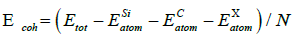
Where  is the cohesive energy;
![]() is the total energy of the doped system;
is the total energy of the doped system;  and
and  are the total energies of free atom Si, C and X (X=La, Ce, Th), and N is the total number of the doping system. Our calculated E coh of La, Ce and Th doped 2D SiC is -6.93 eV/atom, -7.01 eV/atom and -7.08 eV/atom, respectively. It can be seen that the three doped 2D SiC systems show stability.
Results and Discussion
Geometry structure
As shown in Figure 1, after the Si atom of 2D SiC substituted by rare earth atom, the bond lengths of X-C are larger than that of Si-C, the bond angles of Si-C-X near the rare earth atom are not 120° and the regular hexagon honeycomb structure exhibits a slight deformation along the x and y direction. Moreover, the 2D SiC with the shape of wrinkled does not present after substituting Si atoms with rare earth atom.
Table 1 shows the optimized lattice constants of pure and rare earth doped 2D SiC (Fixed axis c). DX-C represents the average distance of the X atom (X=Si, La, Ce, Th) to the nearest C atom, dX-Si represents the average distance between the X atom and the nearest Si atom, dC-C represents the average distance between the C atom and the nearest C atom, and Rx represents the covalent radius of the X atom.
It can be seen from Table 1 that the doping of three rare earth elements makes the lattice constants a and b increase, and all of them cause obvious distortion of the crystal lattice near the doping atoms. The degree of distortion is depended on the type of substituting atoms. Compared with the change of bond length caused by the incorporation of three different rare earth atoms, the lattice distortion caused by doping of La atom is the largest, while the lattice distortion caused by Ce atom doping is the smallest. Compared with the pure 2D SiC, the distance of La-doped 2D SiC, dLa-C, dLa-Si and dC-C increased by 26.4%, 5.66% and 26.2%, respectively. After Ce atom doping, dCe-C, dCe-Si and dC-C increased by 21.01%, 4.38% and 20.01% respectively. Compared with the covalent radius of the doped atoms we can see that the covalent radius difference between Si and the doped atom Ce and Th are both 0.54 Å, which is less than that of La 0.58 Å. Therefore, the lattice distortion caused by La atomic doping is the largest. It can be seen that the degree of the lattice distortion near the impurity atom is mainly influenced by the covalent radius of the substituting atom.
| a(Å) | b(Å) | dX-C(Å) | dX-Si(Å) | dC-C(Å) | Rx(Å) | |
|---|---|---|---|---|---|---|
| 2D SiC | 15.42 | 15.42 | 1.78 | 3.108 | 3.108 | 1.11(Si) |
| La-doped | 15.65 | 15.64 | 2.269 | 3.284 | 3.922 | 1.69 |
| Ce-doped | 15.57 | 15.60 | 2.154 | 3.244 | 3.730 | 1.65 |
| Th-doped | 15.62 | 15.61 | 2.207 | 3.267 | 3.823 | 1.65 |
Table 1: The optimized structural parameters of pure and La, Ce and Th doped 2D SiC.
Electronic structure
Figure 2 shows the band structures near the Fermi energy of pure and La, Ce and Th doped 2D SiC.
Figure 2a show that 2D SiC is a direct band-gap semiconductor with a gap of 2.60 eV [35], and the valence band maximum (VBM) and the conduction band bottom (CBM) are both at the K point in the Brillouin zone. This value is close to the previously reported band gaps of SiC slice of 2.50 eV [36] and 2.55 eV [37].
After doping with different rare earth atom, the band structures of 2D SiC are different. From Figure 2b it can be seen that, when doping with La, impurity energy appeared at the Fermi energy, and the band gap of VBM to the impurity energy is 0.36 eV and the gap of impurity energy to the CBM is 1.93eV. From Figure 2c and Figure 2d, the valence band of Ce or Th doped 2D SiC move down and the band gap narrow down obviously, and they become indirect band structure. But the difference between direct and indirect band gap is very small, they are considered to be quasi-direct band-gap semiconductors. When doping with Ce or Th, the indirect bandgap is 1.53 eV and 1.72 eV, which is 0.03 eV and 0.02 eV smaller than the direct band-gap, respectively. The energy bands number of all doped systems and pure 2D SiC are all have 12 energy bands, but the distribution of energy bands is different, which is derived from the distribution of different electron orbitals of rare earth atoms.

Figure 2: Band structures near the Fermi energy of pure and La, Ce and Th doped 2D SiC
(a) pure 2D SiC (b) La-doped (c) Ce-doped (d) Th-doped.
Figures 3a-3d shows the partial density of states of pure and La, Ce and Th doped 2D SiC. In order to convenient analysis, the range of energy range of the eigenstate and the doped state density is -15 eV to 5 eV, including the upper valence bands (UVB), lower valence bands (LVB) and the conduction bands (CB).

Figure 3: Partial density of states of pure and La, Ce and Th doped 2D SiC (a) pure 2D SiC (b) La-doped (c) Ce-doped (d) Th-doped.
Figure 3a shows that LVB of 2D SiC mainly distribute at -14 ~ -10 eV, and there is a higher density of states (DOS) near -10.72 eV, which is mainly composed of C-2s electrons. UVB distribute at -8 ~ 0 eV, with a higher DOS near -2.83 eV and -0.66 eV, which is mainly composed of C-2p and Si-3p electrons. CB distributes between 2.60 eV and 3.92 eV, and there is a higher DOS near 2.69 eV, which is mainly contributed by Si-3p electrons.
As shown in Figure 3b, after doping La, LVB is mainly composed of C-2s and Si-3s electrons. UVB is mainly composed of C-2p, Si- 3p and La-5d electrons. DOS of C-2p and La-5d through the Fermi energy, which corresponding to the impurity energy in the band structure of La-doped 2D SiC (Figure 2b). CB is mainly composed of Si-3p and La-5d electrons. As shown in Figure 3c, when doping with Ce, the valence band is mainly composed of C-2p and Si-3p electrons, and CB is mainly composed of Si-3p and Ce-4f electrons. As shown in Figure 3d, when doping with Th, the valence band is mainly composed of C-2p and Si-3p electrons, and CB is mainly composed of Si-3p and Th-6s6d5f electrons. Distribution of DOS is completely corresponding to the band structure in Figure 2. To be specific, Th does not contain 5f electrons from the electron configuration, but after the structural optimization, 5f state electrons of Th atom appear in the electron state. It can be speculated that, in the process of the Th atom substituting Si atoms bond with C atoms, Th-7s electron jumps to 5f electron and hybridizes with C-2p, thus reducing the total energy of the doped system.
Charge density difference and population analysis
Charge density difference is the difference of the charge density after bonding and the corresponding atomic charge density. This difference is expressed as Δρ=ρABsc-ρABnsc, where ρABsc is the charge density after bonding and ρABnsc is the charge density before bonding.
This study obtains the interatomic bonding situation, charge distribution, transfer, and chemical properties of the bond in the material system by analyzing the charge density difference and population. The overlap electrons distribute between two atoms called the bond Mulliken population. High bond Mulliken population means high covalent composition, and low bond Mulliken population means high ionic bond component.
Figure 4 shows the distribution of charge density difference of pure and La, Ce and Th doped 2D SiC. Notably, the bond Mulliken population is low in the white area whereas high in the black area.
The electronegativity value of C, Si, La, Ce and Th are 2.55 kJ/mol, 1.90 kJ/mol, 1.11 kJ/mol, 1.12 kJ/mol and 1.30 kJ/mol respectively. Far away from the doped atoms, because C atoms are more electronegative than Si atoms, it is easy for C atoms to get electrons and Si atoms tend to lose electrons. From Figure 4 it can be seen that, there are three large black spots surround C atom, which means the charge accumulation in the region, and Si atoms is surrounded by three small white spots, which means the charge loss in the region. All of the electronegativity values of the three rare earth elements are lower than that of C and Si, after replacing Si atom with La, Ce or Th atom, rare earth atom loses electrons while suppressing Si's electron loss and C's electron gain, which can be seen in Figure 4 and Table 2. As it can be seen in Figure 4b and Figure 4d, after the replacement of Si atoms by La atom, a gray area is presented surround it, indicating that electrons lose in the area. After Ce atom replacing Si atom, the obvious white spots appear in the Ce-C directions, indicating that the electrons density decrease in the Ce-C direction. After Si atom is replaced by Th atom, three off white spots appears in the Th-C directions, and three dark spots surround Th atom. The Th atom is surrounded by black and white alternating regions, which means that not only the charge loss but also the charge accumulation around the Th atoms. This may be related to the Th’s 4f-shell full shell electrons.

Figure 4: (color online) Distribution of charge density difference of pure and La, Ce, Th doped 2D SiC (a) pure 2D SiC (b) La-doped (c) Ce-doped (d) Th-doped.
| Sample | Atom | s | p | d | f | Total | Charge(e) | Atom bond | Population |
|---|---|---|---|---|---|---|---|---|---|
| SiC | C | 1.47 | 3.99 | - | - | 5.46 | -1.46 | C-Si | 0.93 |
| Si | 0.91 | 1.63 | - | - | 2.54 | 1.46 | |||
| La-doped | C | 1.47 | 3.94 | - | - | 5.41 | -1.41 | C-Si | 0.94 |
| Si | 0.94 | 1.68 | - | - | 2.61 | 1.39 | |||
| La | 1.90 | 5.45 | 1.75 | - | 9.10 | 1.9 | La-C | 0.08 | |
| Ce-doped | C | 1.46 | 3.95 | - | - | 5.41 | -1.41 | C-Si | 0.93 |
| Si | 0.93 | 1.67 | - | - | 2.60 | 1.40 | |||
| Ce | 1.92 | 5.45 | 1.83 | 1.06 | 10.26 | 1.74 | Ce-C | 0.13 | |
| Th-doped | C | 1.46 | 3.96 | - | - | 5.42 | -1.42 | C-Si | 0.93 |
| Si | 0.93 | 1.67 | 2.60 | 1.40 | |||||
| Th | 2.03 | 5.47 | 1.95 | 0.66 | 10.11 | 1.89 | Th-C | 0.24 |
Table 2: Atomic orbital and bond population of pure and La, Ce and Th doped 2D SiC.
Table 2 shows the atomic orbital and bond population of pure and La, Ce and Th doped 2D SiC. The value of atomic orbital population, total number of population, the number of effective charges, and the average of the key fabric are the average of each atom, atomic orbital or bond.
As shown in Table 2, the effective charge of each C atom and Si atom in pure 2D SiC is equal to 1.46 e, and the number of C-Si bonds is 0.93, indicating that the C-Si bond contains ionicity. When Si atom is replaced by rare earth atom, the effective charge of each C atom and Si atom reduces to -1.40 e, and the rare earth atoms lose their electrons. After doping with rare earth atom, the C-Si bond essentially unchanged. The bond population values of rare earth atoms and carbon atoms are less than 0.24, which shows that bond of rare earth atoms and C atoms has weak covalent, while ionic is stronger. The population value of the La-C bond is the minimum which shows that the bond cooperation between La-C atoms is the smallest, which is consistent with the result of the difference charge density.
Optical properties
The complex dielectric function, absorption coefficients and complex refractive index of La, Ce, Th doped 2D SiC are calculated.
Figures 5a and 5b shows the complex dielectric function of pure and La, Ce, Th doped 2D SiC (smearing=0.2).

Figure 5: (color online) Complex dielectric function of pure and La, Ce, Th doped 2D SiC (a) Real part ε1 (ω), (b) Imaginary part ε2 (ω).
From Figure 5a it can be seen that the static dielectric constant ε1(0) is 1.60, 2.33, 1.45 and 1.60 for pure 2D SiC and La, Ce, Th doped 2D SiC, respectively. It is clear that doping with La can increase the static dielectric constant of 2D SiC, while Th has little influence to ε1(0). Among the four structures, ε1(ω) of Ce-doped and Th-doped 2D SiC are positive, while for pure 2D SiC and La-doped 2D SiC, ε1(ω) is negative between 3.49 ~ 3.73 eV and 2.97 ~ 3.56 eV, respectively. When ε1(ω)>0, photons propagated in the structure, when ε1(ω)<0, the electromagnetic wave is damped, when ε1(ω)=0, only longitudinally polarized waves are possible.
Figure 5b shows that in the range of 0 ~ 15 eV, ε2(ω) of pure 2D SiC has five peaks (black line and numbers), and the first peak is the strongest peak appears at 3.31 eV, which is come from electron transitions between C-2p and Si-3p. The second to the fifth peaks are located at 4.03 eV, 5.32 eV, 6.95 eV and 10.32 eV, respectively. ε2(ω) of La-doped 2D SiC has six peaks (red line and numbers). The first peak is located at 0.48 eV, which is come from electron transitions between C-2p and La-5d, corresponding to the band gap of VBM to impurity energy. The strongest peak located at 2.86 eV is higher than that of pure 2D SiC. ε2(ω) of Ce-doped 2D SiC has two peaks (blue line and numbers) which located at 3.06 eV and 10.11 eV, respectively. ε2(ω) of Th-doped 2D SiC has three peaks (green line and numbers) which located at 3.06 eV, 6.75 eV and 10.11 eV, respectively. All peaks of ε2(ω) of Ce or Th doped 2D SiC are smaller than the corresponding peaks of pure 2D SiC.
Figure 6 shows the absorption coefficient spectra of pure and La, Ce, Th doped 2D SiC. As shown in Figure 6, the α(ω) of pure 2D SiC is zero in the photon energy of 0 ~ 1.77 eV, 11.42 ~ 12.49 eV, and larger than 16.00 eV. Therefore, pure 2D SiC is completely transparent in the photon energy range above mentioned. It can be seen that pure 2D SiC has three main absorption regions in the ranges of 2 ~ 6 eV, 6.3 ~ 7.5 eV and 9.4 ~ 11 eV. In the visible region of 1.77 ~ 3.26 eV (the corresponding wave length is 700 ~ 380 nm), the maximum absorption peak of pure 2D SiC is located at 3.47 eV, which is the second largest absorption peak in with the corresponding luminousness of 99.84%. The maximum absorption peak 6.79 × 104 cm-1 and second largest absorption peak 5.94 × 104 cm-1 are located at 10.40 eV and 3.47 eV, respectively, with the corresponding wavelengths of 119 nm and 357 nm.

Figure 6: (color online) Absorption coefficients spectra of pure and La, Ce, Th doped 2D SiC.
The α(ω) of La or Th doped 2D SiC has two main absorption regions in the ranges of 0.27 ~ 8.29 eV and 8.79 ~ 13.47 eV (Ladoped), 2.02 ~ 7.37 and 8.77 ~ 13.24 eV (Th-doped). The maximum absorption peak of La or Th doped 2D SiC is 6.32 × 104 cm-1 and 5.16 × 104 cm-1, respectively, which are located at 3.02 eV and 10.18 eV. The α(ω) of Ce-doped 2D SiC has only one absorption region in the range of 1.37 ~ 7.23 eV. The maximum absorption peak of Ce-doped 2D SiC is 6.88 × 104 cm-1 located at 3.40 eV.
Figure 7 shows the complex refractive index of pure and La, Ce, Th doped 2D SiC.

Figure 7: (color online) Complex refractive index of pure and La, Ce, Th doped 2D SiC (a) Refractive index n(ω), (b) Extinction coefficient ú(ω).
As shown in Figure 7a, the refractive index n0 are 1.26, 1.53, 1.35 and 1.26 for pure and La, Ce, Th doped 2D SiC, respectively. The features of ε1(ω) are closely related to the n(ω) of the five structures. Doping Th has little influence on the refractive index of 2D SiC. The present study designs three rare earth doped 2D SiC with refractive index of 1.26 to 1.53, which can provide a new reference for the exploitation of low refractive index materials.
Extinction coefficient ú(ω) indicates light attenuation. For pure and La, Ce, Th doped 2D SiC, the first peaks of ú(ω) are located at 3.44 eV, 0.48 eV, 3.31eV and 3.26 eV, respectively. Compared Figure 7b with Figure 5b, it can be seen that the number of main peaks of ε2(ω) and ú(ω) of 2D SiC, La-doped and Th-doped are same, and the main peaks are located in similar areas, and the trend of the curves are basically the same. For Ce-doped ú(ω), a peak appears only at 3.40 eV, which is consistent with the case of α(ω). The peak of ú(ω) located at about 10 eV disappeared.
Conclusion
The geometry structure, energy band structure, density of states and optical properties of pure and La, Ce, Th doped 2D SiC are investigated by using first-principle method. On the basis of the calculation results, the following conclusions are obtained.
All structures of La, Ce, Th doped 2D SiC can be stable. The structure of 2D SiC shows a slight deformation at the plane direction and the plane structure does not bend after substituting Si atoms with rare earth atoms. The degree of the lattice distortion near the impurity atom is mainly influenced by the covalent radius of the substituting atom.
2D SiC is a direct band-gap semiconductor with a gap of 2.60 eV. After doping with different rare earth atom, the band structure of 2D SiC are all have 12 energy bands, but the distribution of energy bands is different. La-doped 2D SiC imposed an impurity energy at the Fermi energy, and the band gap is 1.93 eV. When doping with Ce or Th, they become quasi-direct band-gap semiconductors.
VBM and CBM of pure 2D SiC are mainly composed of C-2p and Si-3p. After doping with La, Ce and Th, UVB is mainly contributed by C-2p and Si-3p electrons and containing La-5d and Th-6d electrons, respectively. CB is mainly composed of Si-3p electrons, and contains La-5d, Ce-4f and Th-6s6d5f electronics contribution, respectively.
When Si atom is replaced by rare earth atom, the rare earth atoms lose their charges. The bond of rare earth atom and carbon atom has weak covalent, while ionic is stronger.
La-doped 2D SiC has the biggest static dielectric constant 2.33, the biggest peak of ε2(ω) in the low energy region, the maximum refractive index n0 1.53. Ce-doped 2D SiC has the maximum absorption 6.88 × 104 cm-1 in the lower energy region among the four structures. La or Ce doped 2D SiC can enhance the absorption in the range of 0 ~ 5 eV, while Th-doped will decrease the absorption of 2D SiC in the range of 0 ~ 15 eV.
Acknowledgements
Project supported by natural science foundation of Guizhou Province, China (Grant No.(2015) 2001), the innovation team of Anshun university (Grant No.2015PT02), the doctoral fund of Anshun university (Grant No. Asxybsjj201503).
References
- Novoselov KS, Geim AK, Morozov SV, Jiang D, Katsnelson MI, et al. (2005) Two-dimensional gas of massless dirac fermions in graphene. Nature 438: 197-200.
- Berger C, Song Z, Li X, Wu X, Brown N, et al. (2006) Electronic confinement and coherence in patterned epitaxial graphene. Science 312: 1191-1196.
- Zhang YB, Tan YW, Stormer HL (2005) Experimental observation of the quantum hall effect and berry's phase in grapheme. Nature 438: 201-2014.
- Novoselov KS, Geim AK, Morozov SV, Jiang D, Zhang Y, et al. (2004) Electric field effect in atomically thin carbon films. Science 306: 666-669.
- Cahangirov S, Topsakal M, Aktürk E, Ahin HS, Ciraci S, et al. (2009) Two- and one-dimensional honeycomb structures of silicon and germanium. Phys Rev Lett 102: 236804.
- Liu CC, Feng W, Yao Y (2011) Quantum spin hall effect in silicene and two-dimensional germanium. Phys Rev Lett 107: 076802.
- Liu CC, Jiang H, Yao Y (2011) Low-energy effective hamiltonian involving spin-orbit coupling in silicene and two-dimensional germanium and tin. Phys Rev B 84: 195430.
- Feng BJ, Ding ZJ, Meng S, Yao YG, He XY, et al. (2012) Evidence of silicene in honeycomb structures of silicon on Ag(111). Nano Lett 12: 3507-3511.
- Chen L, Li H, Feng B, Ding Z, Qiu J, et al. (2013) Spontaneous symmetry breaking and dynamic phase transition in monolayer silicene. Phys Rev Lett 110: 085504.
- Li L, Lu SZ, Pan J, Qin Z, Wang YQ, et al. (2014) Buckled germanene formation on Pt(111). Adv Mater 26: 4820-4824.
- Lalmi B, Oughaddou H, Enriquez H, Kara A, Vizzini S, et al. (2010) Epitaxial growth of a silicene sheet. Appl Phys Lett 97: 223109.
- Vogt P, De Padova P, Quaresima C, Avila J, Frantzeskakis E, et al. (2012) Silicene: Compelling experimental evidence for graphenelike two-dimensional silicon. Phys Rev Lett 108: 155501.
- Chen L, Liu CC, Feng BJ, He XY, Cheng P, et al. (2012) Evidence for Dirac Fermions in a Honeycomb Lattice Based on Silicon. Phys Rev Lett 109: 056804.
- Meng L, Wang YL, Zhang LZ, Du SX, Wu RT, et al. (2013) Buckled silicene formation on Ir(111). Nano Lett 13: 685-690.
- Fleurence A, Friedlein R, Ozaki T, Kawai H, Wang Y, et al. (2012) Experimental evidence for epitaxial silicene on diboride thin films. Phys Rev Lett 108: 245501.
- Coleman JN, Lotya M, O'Neill A, Bergin SD, King PJ, et al. (2011) Two-dimensional nanosheets produced by liquid exfoliation of layered materials. Science 331: 568-571.
- Zeng ZY, Yin ZY, Huang X, Li H, He QY, et al. (2011) Single-layer semiconducting nanosheets: High-yield preparation and device fabrication. Angew Chem Int Ed 50: 11093-11097.
- Zhang ZH, Guo WL (2008) Energy-gap modulation of BN ribbons by transverse electric fields: First-principles calculations. Phys Rev B 77: 075403.
- Takao Y, Asahina H, Morita A (1981) Electronic structure of black phosphorus in tight binding approach. J Phys Soc Jpn 50: 3362-3369.
- Li LK, Yu YJ, Ye GJ, Ge Q, Ou XD, et al. (2014) Black phosphorus field-effect transistors. Nat Nanotech 9: 372-377.
- Chen SJ, Liu YC, Shao CL, Mu R, Lu YM, et al. (2005) Structural and optical properties of uniform zno nanosheets. Adv Mater 17: 586.
- Sahin H, Cahangirov S, Topsakal M, Bekaroglu E, Akturk E, et al. (2009) Monolayer honeycomb structures of group-IV elements and III-V binary compounds: First-principles calculations. Phys Rev B 80: 155453.
- Zhou LJ, Zhang YF, Wu LM (2013) SiC2 Siligraphene and nanotubes: Novel donor materials in excitonic solar cells. Nano Lett 13: 5431
- Y Ding, Y Wang (2014) Geometric and Electronic Structures of Two-Dimensional SiC3 Compound. J Phys Chem C: 118: 4509.
- Shi Z, Zhang Z, Kutana A, Yakobson BI (2015) Predicting two-dimensional silicon carbide monolayers. ACS Nano 9: 9802-9809
- Chabi S, Chang H, Xia Y, Zhu Y (2016) From graphene to silicon carbide: Ultrathin silicon carbide flakes. Nanotechnol 27: 075602.
- Dar A, Majid A (2013) Electronic structure analysis of rare earth ions Ce and Nd doped gallium nitride. J Appl Phys 114: 123703.
- HL Li, Z Zhang, YB Lu, JZ Huang, Y Zhang, et al. (2013) First principles study on the electronic and optical properties of ZnO doped with rare earth. Acta Phys Sin 62: 047101.
- QQ Li, QY Hao, Y Li, GD Liu (2013) Theory study of rare earth (Ce, Pr) doped GaN in electronic structrue and optical property. Acta Phys Sin 62: 017103.
- Segall MD, Lindan PJ, Probert MJ, Pickard CJ, Hasnip PJ, et al. (2002) First-principles simulation: Ideas, illustrations and the CASTEP code. J Phys: Condens Matter 14: 2717-2744.
- Perdew JP, Burke K, Ernzerhof M (1996) Generalized gradient approximation made simple. Phys Rev Lett 77: 3865
- Vanderbilt D (1990) Soft self-consistent pseudopotentials in a generalized eigenvalue formalism. Phys Rev B 41: 7892.
- Monkhorst HJ, Pack JD (1976) Special points for brillouin-zone integrations. Phys Rev B 13: 5188
- Medeiros PV, de Brito Mota F, Mascarenhas AJ, de Castilho CM (2010) Adsorption of monovalent metal atoms on graphene: A theoretical approach. Nanotechnol 21: 115701.
- WJ Yan, Q Xie, XM Qin, CH Zhang, ZZ Zhang, et al. (2017) First-principle analysis of photoelectric properties of silicon-carbon materials with graphene-like honeycomb structure. Comput Mater Sci 126: 336.
- Zhou YG, Yang P, Wang ZG, Xiao HY, Zu XT, et al. (2011) Functionalized graphene nanoroads for quantum well device. Appl Phys Lett 98: 093108.
- Huda MN, Yan Y, Al-Jassim MM (2009) On the existence of Si-C double bonded graphene-like layers. Chem Phys Lett 479: 255-258.

